Here's a power supply that has dual tracking positive/negative outputs plus a third independent positive output using common and inexpensive LM317 and LM337 three-terminal regulators, with all outputs being adjustable down to zero volts.
This is useful for powering logic circuits from the independent positive output, along with the dual positive/negative outputs for any analog circuits.
The output of an LM317 is nominally 1.25V greater than the ADJ pin, thus the minimum output is 1.25V if the ADJ pin is connected to ground.
The circuit below adds an additional LM337 (U3) to generate a -1.25V reference voltage for U1's and U7"s ADJ terminal, allowing their outputs to be adjusted to 0V output.
For the dual outputs (+Vt, -Vt), the positive output is mirrored by the op amp to U4's LM337 ADJ input, so that the minus output tracks the positive output, allowing the negative output to go to 0V also.

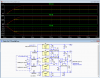
The input consists of a 15Vac center-tapped transformer going to a bridge rectifier and filter to generate ≈±20Vdc.
Regulator U2 provides +4V for the op amp positive power.
The maximum positive U2 output is +1.25V for a 0V supply output so U2's plus supply voltage only has to be large enough to accommodate that.
The plus op amp power can't be the bridge voltage because that would exceed the op amps voltage rating.
The simulated voltage across the op amp for the circuit shown is about 25V.
The simulation shows the output voltages for U5's and U8's pot position of 0%, 50%, and 100%.
As the output voltage of U1 is varied by the pot, op amp U6 adjusts the voltage at U4's ADJ pin to keep the voltage at the junction of resistors R3 and R6 equal to 0V (common).
Since R3 equals R6, the minus output must equal the plus output (within the tolerance limits of the resistor values) to maintain this junction at 0V.
Note that if it is desired to have the plus and minus at different voltages; or to be able to adjust the two voltage magnitudes to be exactly equal, R3 and R6 can be replaced by optional pot U9 with the wiper connected to opamp U6's minus input (dotted lines).
This will change the minus voltage ratio with respect to the positive voltage.
The voltages will then track at this ratio when pot U5 is adjusted.
The minimum voltage of each output depends primarily upon the tolerance of the various regulator 1.25V reference voltages, but the worst-case zero volt level should be no more than ±100mV from 0V, which should be adequate for all but the most critical applications.
Only U1, U4 and U7 will dissipate significant power, depending upon the output current, so are the only ones that need to be on a heatsink.
The dissipation of each regulator is equal the input minus the output voltage times the current, so can become quite high for low output voltages and higher current levels. You may want to consider a fan-cooled heatsink such as used to cool PC CPU chips.
A transformer with different output voltages can be used as long as the maximum voltage rating of the op amp is not exceeded (32V for the LM324/358).
The transformer's output RMS current rating should be at least 1.6 times the sum of the maximum desired output current of the three outputs. This derating is required due to the high RMS peak currents that a rectifier-capacitor filter causes in the transformer.
To minimize the effects of wire resistance on the output voltage regulation due to output current, the tops of resistors R7 and R1, and the bottom connection for R6 should be connected directly to the respective regulator's output pins, separate from the connection for the output wire (and definitely do not connect to the supply output connector terminal). The reason for this is any resistance between the output terminals and the connection for these resistors will significantly degrade the voltage regulation.
For example a 10mV drop between the output pin and the sense resistor connection will drop the output voltage by 0.8%.
But opposite to that, the common connection for U3 and the (+) pin of U8 should be connected directly to the supply output common terminal for best regulation.
This is useful for powering logic circuits from the independent positive output, along with the dual positive/negative outputs for any analog circuits.
The output of an LM317 is nominally 1.25V greater than the ADJ pin, thus the minimum output is 1.25V if the ADJ pin is connected to ground.
The circuit below adds an additional LM337 (U3) to generate a -1.25V reference voltage for U1's and U7"s ADJ terminal, allowing their outputs to be adjusted to 0V output.
For the dual outputs (+Vt, -Vt), the positive output is mirrored by the op amp to U4's LM337 ADJ input, so that the minus output tracks the positive output, allowing the negative output to go to 0V also.
The input consists of a 15Vac center-tapped transformer going to a bridge rectifier and filter to generate ≈±20Vdc.
Regulator U2 provides +4V for the op amp positive power.
The maximum positive U2 output is +1.25V for a 0V supply output so U2's plus supply voltage only has to be large enough to accommodate that.
The plus op amp power can't be the bridge voltage because that would exceed the op amps voltage rating.
The simulated voltage across the op amp for the circuit shown is about 25V.
The simulation shows the output voltages for U5's and U8's pot position of 0%, 50%, and 100%.
As the output voltage of U1 is varied by the pot, op amp U6 adjusts the voltage at U4's ADJ pin to keep the voltage at the junction of resistors R3 and R6 equal to 0V (common).
Since R3 equals R6, the minus output must equal the plus output (within the tolerance limits of the resistor values) to maintain this junction at 0V.
Note that if it is desired to have the plus and minus at different voltages; or to be able to adjust the two voltage magnitudes to be exactly equal, R3 and R6 can be replaced by optional pot U9 with the wiper connected to opamp U6's minus input (dotted lines).
This will change the minus voltage ratio with respect to the positive voltage.
The voltages will then track at this ratio when pot U5 is adjusted.
The minimum voltage of each output depends primarily upon the tolerance of the various regulator 1.25V reference voltages, but the worst-case zero volt level should be no more than ±100mV from 0V, which should be adequate for all but the most critical applications.
Only U1, U4 and U7 will dissipate significant power, depending upon the output current, so are the only ones that need to be on a heatsink.
The dissipation of each regulator is equal the input minus the output voltage times the current, so can become quite high for low output voltages and higher current levels. You may want to consider a fan-cooled heatsink such as used to cool PC CPU chips.
A transformer with different output voltages can be used as long as the maximum voltage rating of the op amp is not exceeded (32V for the LM324/358).
The transformer's output RMS current rating should be at least 1.6 times the sum of the maximum desired output current of the three outputs. This derating is required due to the high RMS peak currents that a rectifier-capacitor filter causes in the transformer.
To minimize the effects of wire resistance on the output voltage regulation due to output current, the tops of resistors R7 and R1, and the bottom connection for R6 should be connected directly to the respective regulator's output pins, separate from the connection for the output wire (and definitely do not connect to the supply output connector terminal). The reason for this is any resistance between the output terminals and the connection for these resistors will significantly degrade the voltage regulation.
For example a 10mV drop between the output pin and the sense resistor connection will drop the output voltage by 0.8%.
But opposite to that, the common connection for U3 and the (+) pin of U8 should be connected directly to the supply output common terminal for best regulation.