Continue to Site

Welcome to our site!

Electro Tech is an online community (with over 170,000 members) who enjoy talking about and building electronic circuits, projects and gadgets. To participate you need to register. Registration is free. Click here to register now.

  • Welcome to our site! Electro Tech is an online community (with over 170,000 members) who enjoy talking about and building electronic circuits, projects and gadgets. To participate you need to register. Registration is free. Click here to register now.

ZVS Driver but in reverse

Status
Not open for further replies.

codex653

New Member
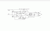
i was thinking about different things for switching supplies, and the ZVS driver came to mind from a different HV project i had had before, specifically the mazilli driver.....an interesting idea came to mind about running it in reverse so as to take a higher voltage (mains) down to a usable voltage or voltages for projects. I've built the mazilli driver before as shown here:

**broken link removed**

but that was with a lower supply voltage....if i ran this thing off of rectified mains i imagine quite a few changes would have to be made! one of the main problems i see is spikes coming back from the transformer since i had to deal with that the first time around.

what do you all think of this? sounds like an interesting project huh!
 
hehe check it out! :D i think i may have just redesigned the Mazzilli ZVS flyback driver to work in reverse! haha...by that i mean so that i can use it as a step down transformer that is run off of rectified mains! :) I feel excited cause i think it might work! but then again i'm nowhere near an electrical engineer so my ideas just might go ka-poof :p

anyways, this is the original Mazzilli:

**broken link removed**

my redesigning schematic i have tried posting in this thread..i hope it showed up :p EDIT: oh ok yah it did...it's at the bottom of this post :)

so here are some notes that i took while designing it :)

-R1 and R3 dissipate 0.256 W
-R2 and R4 dissipate 0.025W
-R1 and R2 form a voltage divider so that 16v at 1mA is at the base of the BU4525AX
-I feel like i will most likely be needing to have a transistor before the BU4252AX's so as to provide more current to the base...the gain is only 12, and i am looking for around a 2A current flowing through the primary so as to get 320 watts since this would be supplying my 150 watt RMS amp (i'm accounting for worst case power dissipation on the amp chip IC)...i don't think that 1mA is enough base drive current.
-I don't need the zener diodes because, as far as i know, they are only used to clamp the voltage to the base/gate (depending on which diagram you are looking at) to 12v.
-D1-D4 are used for voltage spike suppression
-I do not know at all what the purpose of C1 is for....a snubber type of thing?? or maybe resonance?
-BU4525AX have a 800v rating, so that can easily handle the high voltages being used, PLUS it has a fast switching time of only 1 or 2 microseconds!:)
-I still have yet to determine the value of the inductor...as i understand it, its purpose is used to limit the current.

so...what do you think?? is this practical? or am i just way out there, and this won't even come close to working?
 

Attachments

  • Reverse Mazzilli.gif
    Reverse Mazzilli.gif
    12.4 KB · Views: 1,387
Last edited:
Status
Not open for further replies.

Latest threads

New Articles From Microcontroller Tips

Back
Top