Continue to Site

Welcome to our site!

Electro Tech is an online community (with over 170,000 members) who enjoy talking about and building electronic circuits, projects and gadgets. To participate you need to register. Registration is free. Click here to register now.

  • Welcome to our site! Electro Tech is an online community (with over 170,000 members) who enjoy talking about and building electronic circuits, projects and gadgets. To participate you need to register. Registration is free. Click here to register now.

Why the dip?

Status
Not open for further replies.

jpanhalt

Well-Known Member
Most Helpful Member
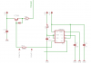
The oscilloscope tracings shown below are circuit at R12, which is the base drive for an NPN output transistor. I have omitted some aspects of the circuit for clarity.

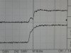
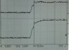
The TOP oscilloscope tracing (50 nS sweep) is taken at Point B (“after” R12); the BOTTOM tracing is taken at Point A (“before" R12).

Why is there a dip in the tracing made at Point B (after R12)?

Thanks. John
 

Attachments

  • Base Drive.png
    Base Drive.png
    7.9 KB · Views: 649
  • base dip NPN drive_sm.jpg
    base dip NPN drive_sm.jpg
    178.6 KB · Views: 456
Does using the different diode change the timing of the DIP?
 
I did not carefully measure the timing of the dip; however, the dip looks to be about the same with or without the diode. I did not try different diodes, like Schottky. I also tried a Baker clamp (base to collector diode), larger bypass caps on the 555, larger cap at C10, and higher R for R14, but those changes had no or very little effect either.

It seems the base in FZT851 is turning on at different rates, e.g., a larger area abruptly starts to conduct shortly after initial turn-on. On Semiconductor has an application note (AN875) that seems to address that issue, i.e., the need for more base current shortly after start of turn-on. It suggests a snubber, but doesn't give any more information on the configuration.
John
 
It's due to the Miller effect. While the transistor is in the active region, it has a lot of gain, so the effective collector-base capacitance looks much larger than it actually is. Seen on a perfect scope, with a perfect probe with zero inductance, it would look like a (nearly) flat spot.
EDIT: OOps! I thought that I was looking at a common emitter stage. Disregard my comments.
 
Last edited:
I added a some capacitance (200 to 800 pF) to ground on the gate (like a low pass filter). The dip disappeared, but of course, the whole trace flattened.

Would a Darlington perform better (i.e., as fast switching with no dip)? What are some of the reasons not to use a Darlington? John
 
I think the dip occurs because the base-emitter capacitance is not bootstrapped until the base voltage gets high enough that the emitter can follow it. Once that happens, the effective base capacitance is reduced, being mostly just collector-base capacitance. Since the emitter voltage follows the base voltage with near-unity gain, very little charge has to flow into the base-emitter capacitance once the transistor is active.
You don't generally need a base resistor on an emitter follower. Try removing it, if the dip bothers you.
 
Roff said:
You don't generally need a base resistor on an emitter follower. Try removing it, if the dip bothers you.

I put it in to limit current from the 555 to less than 200 mA. The load will just be a pulse around 1 mS, repeated at most every 4 to 10 seconds. Would you anticipate any problem with such an arrangement? It's built using SMD, so putting a zero ohm across it will be quite easy as a test. I will let you know what happpens.

Would you leave the diode as shown, connect it to the collector (to mitigate potentially over driving the base), or eliminate it altogether? The load is a 90A SCR used in a capacitance discharge spot welder, and I put the resistor in initially as protestion from reverse biasing the emitter-base with any spikes. On the scope trace of the test circuit using only minimal current to keep the SCR conducting, not the full weldiing current, the emitter stays below the base voltage.

Thanks. John
 
jpanhalt said:
I put it in to limit current from the 555 to less than 200 mA. The load will just be a pulse around 1 mS, repeated at most every 4 to 10 seconds. Would you anticipate any problem with such an arrangement? It's built using SMD, so putting a zero ohm across it will be quite easy as a test. I will let you know what happpens.

Would you leave the diode as shown, connect it to the collector (to mitigate potentially over driving the base), or eliminate it altogether? The load is a 90A SCR used in a capacitance discharge spot welder, and I put the resistor in initially as protestion from reverse biasing the emitter-base with any spikes. On the scope trace of the test circuit using only minimal current to keep the SCR conducting, not the full weldiing current, the emitter stays below the base voltage.

Thanks. John
It's an emitter follower. The emitter voltage will always be below the base voltage, and the 555 can never drive the base above the collector. The base current is basically the emitter current divided by beta+1. Since the emitter current is less than 500mA, and the minimum beta is 100, your 555 output current should never exceed 5mA, except on the transitions. 555s can easily handle short current spikes, so even if they do exceed 100mA, they won't cause a problem.
I would use a 470 ohm resistor from gate to cathode on the SCR, and get rid of the diode. The gate does need a path to ground for leakage current, and the diode doesn't do a good job of that.
EDIT: Is you welding load in the cathode circuit, or the anode? What is your welding supply voltage? If it is higher than +12V, I would put the load in the anode. In fact, I would do that in either case.
 
Last edited:
It worked! Removing the resistor, that is. Thanks, Ron.
The bottom tracing in the attachment is how it looks now.

I did not expect the emitter to go above the base without another factor. That factor was inductive kick from the welder. How it would get from the leads through the gate and back to the transitor, I don't know. It was just over caution. (Most of my experience has been with TIG, and the HF there goes everywhere, which obviously is not the situation here.) But, since the PCB is made, there is no problem leaving it off and adding later, if needed.

Stupid me, I calculated the potential base current
using a higher peak emitter current. I used the transistor rating (did I say dumb?), not the actual, realized it was getting close to the max for the 555, and threw the resistor in to limit it. Obviously, it limited it, and then I spent all of this time trying to avoid that limit without rethinking the original, wrong assumption. The peak emitter current should be a bit more than 500 mA as drawn (i.e., 12 V through 10 ohm). If I go to a 20 ohm gate resistor, then I will be back in the ballpark of 500 mA.

As for the resistor from the SCR gate to the cathode, the SCR I am using is not a sensitive gate one, if I read the datasheet correctly. It is an SKKT92. Do you think the resistor may still be needed?

The SCR will be in the cathode lead of the welder, based on the design link posted by Pommie a couple of weeks ago (https://www.philpem.me.uk/elec/welder/). I don't anticipate going above 12V, but have made the prototype so that I could do that, if needed for the SS tubing I am trying to weld.
John
 

Attachments

  • Base drive_no R.jpg
    Base drive_no R.jpg
    112.4 KB · Views: 235
The link didn't work.
I would use the gate-cathode resistor. It only uses a couple of milliamps, and is good insurance.
 
realisticly what could i build a spot welder for in US dollars. ive been thinking about rebuilding battery packs but find the welders out of my reach to start
 
realisticly what could i build a spot welder for in US dollars. ive been thinking about rebuilding battery packs but find the welders out of my reach to start

It depends on how good a shopper you are and what spare parts you might have at home. The essentials are: 1) A variable DC supply -- plan on needing 18 to 20 volts; 2) large capacitor of 400,000 uF or more -- car audio is fine, but limits voltage on the high side (some are rated at 20V/24 surge); 3) An SCR; 4) a gate switch/relay for the SCR and charger; 5) electrodes, welding cable, and connectors.

Costs:

#1 = Unknown. My first prototype used a variac and a battery charger transformer-bridge rectifier that I had on hand. You can run directly from the variac and bridge rectifier. Just be sure to disconnect the variac before discharging the capacitors or you will blow its fuse. The variac is expensive to buy. A variable DC supply of a few amps could probably be built for about $20.
#2 = I got an used audio cap for $10, most are bit more. Computer caps run about $4 to $5 each for 36,000 uF, of which you need about 12. 18V will be fine for battery tabs in my experience.
#3 = EBay $10
#4 = <$10
#5 = cable (>=4awg) $15; connectors $4; electrodes -- I used 1/4" copper rod that I had, perhaps $10 if yo have to buy it.

So, $50 to $75 total, if you a shop around.

As previously stated, you should start your own thread with a more informative title, should you want to pursue this line of thought.

John
 
Last edited:
Status
Not open for further replies.

Latest threads

New Articles From Microcontroller Tips

Back
Top