Continue to Site

Welcome to our site!

Electro Tech is an online community (with over 170,000 members) who enjoy talking about and building electronic circuits, projects and gadgets. To participate you need to register. Registration is free. Click here to register now.

  • Welcome to our site! Electro Tech is an online community (with over 170,000 members) who enjoy talking about and building electronic circuits, projects and gadgets. To participate you need to register. Registration is free. Click here to register now.

Square Wave Based Inverter (Switch Mode)

Status
Not open for further replies.

C47

New Member
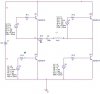
I am building this circuit (12DC to 12VAC) and I am having problems, first of all for the VPULSE, what should I use, a 555 timer or ua741 opamp to create a square wave....

the bigger problem is how many independant vpulse should i have....two are still managable but four are very difficult to syncronize

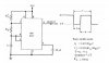
im pretty much late (for my project) here so dont post any more complicated inverter designs..

i removed the protection diodes for the time being....
 

Attachments

  • Circuit.jpg
    Circuit.jpg
    29.5 KB · Views: 1,329
Welcome to the site. C47.
It would be better to use 555 followed by buffers to get more outputs of the same signal. If you want complimentary outputs , you may use 55 at double the frequency, divide it by2 and use the "Q" and "/Q" outputs. By the division method, you achieve 1:1 pulse ratio.
 
Last edited:
thankyou sarma,


tha complimentary idea is billiant if it is in the chip itself....

the problem with the 555 timer is also that is starts with 48Hz and climbs upto 52Hz , ie for some reason its not stable

Im using the NE555P and its doesnt have the Q'...please help
 

Attachments

  • 555P.jpg
    555P.jpg
    8.3 KB · Views: 926
Last edited:
C47 said:
the problem with the 555 timer is also that is starts with 48Hz and climbs upto 52Hz , ie for some reason its not stable

Im using the NE555P and its doesnt have the Q'...please help

hi,
Its not just the Vx drive pulse generator thats the problem.

V4/5 are in opposite phase as are V2/3. Alternating.!

V2 and V5 need to be ON at the same time, with V3 and V4 OFF, then on the next cycle,
V2/5 OFF and V3/4 ON.

The problem arises using 555 is the level shifting for the V2 and V3 pulses as they are not referenced to 0V.

Summary:

Only two phases, but V2 and V3 need level shifting.

Do you follow.?

EDIT: I am assuming that you require the 12Vac across the inductor.???

With ref to the 555 osc frequency drift, please post your circuit, what R,C type components are you using.?
 
Last edited:
ericgibbs said:
hi,
The problem arises using 555 is the level shifting for the V2 and V3 pulses as they are not referenced to 0V.

Summary:

Only two phases, but V2 and V3 need level shifting.

Do you follow.?

the problem is of the GND.....please stay and tell me:

what you mean by level shifting and if i manage to do that what should i do with the GNDS of V2 and V3? where should i put them....at the emitters of the top BJTs?

also are you suggesting to use one 555 timer? coz thats not possible becoz of gnd connections...
 
ericgibbs thankyou for helping.....

as for your reply to the edit:

well the capacitor and inductor were kind of loads...filters sort of things....please excuse my ignorance....i can run the circuit in PSpice with R as a load only too....but the problem is implementing it in real life
 
C47 said:
the problem is of the GND.....please stay and tell me:

what you mean by level shifting and if i manage to do that what should i do with the GNDS of V2 and V3? where should i put them....at the emitters of the top BJTs?

also are you suggesting to use one 555 timer? coz thats not possible becoz of gnd connections...

This what I said.

See edit to my last post.
 
the 555 circuit:

Ra = 1kohm
Rb = 51K+91K
C = 0.1uF

and the 0.01uF is the same as in my circuit

ericgibbs please suggest how many 555 should i use?

DUTY Ratio = 49%

EDIT: I didnt use Pspice for the 555 i just tested it manually and changed RB with a potentiometer when i got 50Hz i put in a fixed resistor
 

Attachments

  • 555 circuit.jpg
    555 circuit.jpg
    31.8 KB · Views: 572
Last edited:
hi C47,

The original circuit, must you follow that design using those types of transistors.

The top two are connected as emitter followers and the bottom two as common emitter. The top two should be pnp transistors.

Is it permitted to change the original design.?
 
ericgibbs said:
hi C47,

The original circuit, must you follow that design using those types of transistors.

The top two are connected as emitter followers and the bottom two as common emitter. The top two should be pnp transistors.

Is it permitted to change the original design.?

well as long as it works.....but i dont see how pnp for the top two would help...what about the GNDs then...will they be connected to the pnp collectors?
 
C47 said:
well as long as it works.....but i dont see how pnp for the top two would help...what about the GNDs then...will they be connected to the pnp collectors?

I'll post a drawing, shortly.:)
 
hi C47,
This is a very basic circuit in order to demonstrate the idea.

As its a 'project' it would best if you calculated the required values.:)

Do you follow it OK.?
 
Last edited:
well what are those empty boxes and where did the 12V go?

and whats the red transistor for?

and where are the drives for the top two?

is this a half bridge rectifier?

EDIT : is this supposed to get rid of syuncronization issues
 
Last edited:
C47 said:
well what are those empty boxes
They are resistor symbols

and where did the 12V go?
Its not gone anywhere, look at your original circuit.

and whats the red transistor for?
inversion of the output from the 555

and where are the drives for the top two?
thru the linking resistors

is this a half bridge rectifier?
No

EDIT : is this supposed to get rid of syuncronization issues
It does get rid of the sync problem

hi C47,
What college year is this project for.?:rolleyes:
 
well for q3 i will use an opamp inverter, is that okay?

im sorry i didnt understand the linking resistor part?

is the red 5V suuposed to be 12V or is it part of the BJT inverter that you meant to use?
 
C47 said:
well for q3 i will use an opamp inverter, is that okay?
Thats OK, something better than a 741 if possible.

im sorry i didnt understand the linking resistor part?
No problem, its easier to draw a rectangular box than a zigzag resistor.:)

is the red 5V suuposed to be 12V
On your drawing you show a 555 with a 5V supply, I was just trying to keep the drive transistor the same.

or is it part of the BJT inverter that you meant to use?
It just powers the invertor.[/QUOTE]

What college year is this project for.?

Hi,
If its easier the 555 can run at 12V, as can the BJT invertor, just calculate the appropiate resistor values.
 
Last edited:
im simulating it in pspice i will use vpulse instead of 555, so its faster and its 14V (sorry my mistake) so that the bjts can operate in switch mode
 
i just popped the 555 when i connected to output to base of the red transistor....are you sure of your circuit?
 
C47 said:
i just popped the 555 when i connected to output to base of the red transistor....are you sure of your circuit?

Yes Im sure.

What value of resistors do you have in the 555 output to the transistor and opa invertor.?

EDIT: post a drawing with the component values on.
 
Last edited:
hi,
Double checked my circuit, OK

If you have popped the 555 you have connected something incorrectly.

Check the supply to the 555 timer make sure its not greater than 15V or so volts, also the connections to the 555, especially pin #3.
 
Status
Not open for further replies.

Latest threads

Back
Top