Electro Tech is an online community (with over 170,000 members) who enjoy talking about and building electronic circuits, projects and gadgets. To participate you need to register. Registration is free. Click here to register now.
Welcome to our site! Electro Tech is an online community (with over 170,000 members) who enjoy talking about and building electronic circuits, projects and gadgets. To participate you need to register. Registration is free. Click here to register now.
Being awakened by a dream of a hot transistor chasing after me I had to look at this circuit a bit closer.
While I was thinking Vce(sat) of 2N4403 (or similar) is 1.1v, it is actually 0.75v. That means the load transistor does not need as much voltage across it.
Consider this: Vbe(on)=0.65, (Vbe will settle at 0.65V for setting transistor while load transistor levels off at 0.75v), Vbe(sat)=0.75, Vce(sat)=0.75, Constant current sink for WS2811 being 18-18.5ma per channel, and if we want to drive each LED color at 300ma (approx.)
Let's set Irws=18ma, and Rws=10 ohms, then Vrws=0.18V, Ve1(load tansistor)=0.18+0.75=0.93v @ current of 288ma gives us 268mw disspipation! With our recent pcb updates we should be good to go.
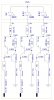
This change will lower Ve2 to 1.59V and hence require a bit higher resistors as Rx (series resistors to RGB). Working backwards Red Resistor becomes about 14.7 ohms, Grn/Blu Resistors become 2.7 ohms.
See new schematics attached.
If we change Irws to 18.5ma, all the voltages increase by 5mv and hence voltage across each color LED drops by 5mv which would be inline with reducing I-led from 350ma to 300ma compared to HP RGB data sheet. This slight change in voltage changes the power dissipation of load transistor to roughly 270mw which is way below maximum power rating (625mw) of the transistors (2N4403).
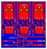
Note the tab needs to be soldered to the heat sink. So I cleared the solder mask off for the tabs. Maybe should be a larger area.
Look at the FZT792A. View attachment 98475
I updated the smd pcb. see above. Upper tab of top SMD Q is the Collector and will be soldered in to top copper (in this case the ground plane). The tab is there, it is just hidden by other layers. For me to show you different layers I have to create individual layers separately otherwise other layers will mask over them.
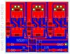
Please note the changes in thru-hole schematics and PCB. I was able to drop the power dissipation of load transistor to 242mw! This compared to 2N4403 datasheet is less than half the power rating of 625mw. If SMD version is around 625mw, then you may not need a significant copper pad or require a heat-sink!
This configuration of two PNP transistors create a negative feedback to each other keeping the currents and voltages in-check. Both transistors come to a rapid equilibrium.
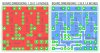
Circuit Simulation and Calculations (Please see attached diagram):
Known: In this configuration Setting Transistor (Q1) is driven in "Just ON" while Load Transistor (Q2) is driven in "Saturation" modes.
Datasheet for Q1 & Q2: 2N4403 TO-92 Package, Ic(max)=600ma, Vbe(on)=0.65v, Vbe(sat)=0.75, Vce(sat)=0.85, Pd=625mw
Datasheet for WS2811: Constant Current Output (Sink) at 18.5ma
Datasheet for HP RGB 10W: Vf(red)=6v, Vf(grn)=9.6v, Vf(blu)=9.6v, I-led (max)=350ma (We are driving the LED's at 300ma, Vcc=12v)
Evaluation: Since Q1 is driven at ON status then its Vbe=0.65v, Q2 is driven at Saturation then its Vbe=0.75v and Vce=0.85v (min)
1- Since Vce2=0.85v and Vbe=0.75v then V1=0.85-0.75=0.1v. We also know Iws=18.5ma hence Rws=0.1/0.0185= 5.4 ohms
2- Since Vce2=0.85v then V2=Vce2=0.85v
3- Since Q1 is in On status, Vbe1=0.65v. Therefore V3=V2+Vbe1=0.85+0.65=1.5v
4- Vx(red)=Vcc-Vf(red)-V3=12-6-1.5= 4.5v, we also know Vx=Rx * I-led therefore Rx=4.5/0.3= 15 Ohms
5- Vx(grn)=Vcc-9.6-1.5= 0.9v then Rx=0.9/0.3= 3 Ohms
6- Vx(blu)=Vcc-9.6-1.5= 0.9v then similarly Rx= 0.9/0.3= 3 Ohms
7- Looking up the datasheet of 2N4403 we note that Ib1(on)= 1.5ma and at this current hfe1=10.3= Ic1/Ib1 then Ic1= 15.5ma and Ie1= 17ma, Is= 283ma
Approx.: Ie1=0.057 x (I-led) and Is= 0.943 x (I-led), (I-led)=Ie1+Is
8- Vs=Voltage across setting resistor, Vbe1=0.65=Is*Rs. Rs=0.65/0.283= 2.3 Ohms
9- Power Dissipation Calculation:
Pq1=Vce1*Ie1=1.4x.017= 23.8mw, Pq2=Vce2*Ie2=0.85x(0.283+.0015)= 242mw, Prs=Vs*Is=0.65x0.283= 184mw
Prws=V1*Iws=0.1x0.0185= 2mw, Prx(red)= Vrx*(I-led)= 4.5x0.3= 1.35W, Prx(grn)=Prx(blu)= 0.9x0.3= 270mw. Recommended Power Rating for Rx(red)=2W, Rx(grn)=Rx(blu)= 0.5W
There are things I don't know. I believe the bottom of the 5.4 ohm resistor will not be at ground. Because there is a constant current source inside the IC the output can not pull to ground. I don't know but I think it will be 0.7 volts minimum. (big guess) Can't fine the number. You might have to turn on the IC and see what happens. Apply a resistor to +12V (15mA load) so the IC will pull down as hard as it can to try to get 18.5mA. Measure the voltage. Inside the IC there must be a resistor to measure current. Some voltage must be across this resistor to measure current. (maybe 1/2 volt) (maybe 0.7V) There is a transistor much like your Q2 but NPN that also has some voltage across it.
Now that the transistor can handle watts, I think the resistor below the LED could be left off.
Today we say a 10% change in LED voltage from 25C to 85C. Is this in your calculations. The voltage was rated at 1.7V but the maximum could be as much as 2.5V and as little as (they did not say). Now I know you will rarely see 2.5V but the LED is still "good" at that voltage.
Have you breadboarded this? I am asking hard questions.
There are things I don't know. I believe the bottom of the 5.4 ohm resistor will not be at ground. Because there is a constant current source inside the IC the output can not pull to ground. I don't know but I think it will be 0.7 volts minimum.
I ordered parts to build it. However I have a different take on Ws chip. I believe they used a high speed, low On-Resistance NMOS (0.1 ohms). This internal resistance would dictate the voltage drop. Again like you I am guessing if such high tech, high speed PWM device may not be as inefficient as you assume it to be! If my guess is correct Vdrop=0.0185x0.1=0.2mv which is too insignificant to worry about. We will know once it is tested.
I wanted to show how the values were calculated. If any major drops is discovered then all Rx's can be adjusted to compensate.
Today we say a 10% change in LED voltage from 25C to 85C. Is this in your calculations. The voltage was rated at 1.7V but the maximum could be as much as 2.5V and as little as (they did not say). Now I know you will rarely see 2.5V but the LED is still "good" at that voltage.
Please see my previous notes regarding voltage and current fluctuations and how negative feedback will bring the system back to equilibrium to compensate. Once again it is worth mentioning that although we set initial voltages for operation, the device will keep a constant current thru the LED. See my next post for a new configuration that addresses Vdrop of WS and any fluctuations in Vf and If due to heat and how system will recover and compensate.
Regards,
Rom
A new version:
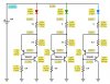
To address the unknown voltage drop of sinking constant current of WS2811, I reconfigured the layout to be almost independent of voltage drop of WS. (i.e.: in case WS's output does not pull down all the way to ground).
I had to do this on the run and produce it in PDF since converting it to an image was losing the details of the text.
In this circuit WS controlls Ic of Q1 and not the base creating somewhat an isolation. Rb is used to pull base of Q1 up a bit. The load current goes thru Q2 now and constant current of WS sets the flow of current thru Rs (changed because of higher current).
If WS voltage drop is increased by 0.7v then V2 is only effected by 1mv (insignificant change) considering part tolerances are 1 to 5%.
If Vf (LED voltage) goes up by 10%, If(led current) will increase by 8.3%, since the system is maintaining a constant current, all the voltages will increase and all the currents will drop to compensate, this pulls the current of LED back down, causing the LED voltage to drop. Since we are maintaining a constant current voltage fluctuation of LED will not effect the system while it maintains a constant current thru the LED.
Inversely if the voltage across LED drops, the LED current drops, voltages pull up, currents increase and system will instantly come to an equilibrium.
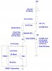
New Design V3:
This diagram has the WS2811 equivalent in the design. Noticed V2 only changed by 0.001v. The Vrb along with Vbe1 are clamping V2 to saturation point of Vce. Hence causing voltage drop of WS2811 to have no significant effect. The equivalent circuit for WS does maintain 18.5ma constant current. I had to build it in simulation before adding it to the main circuit.
I have been looking at the original simulation. It is a LED driver but it is not a constant current. The PNP transistors do not allow for the current to be capped and it will ramp continuously even though supply voltage does not change. However the device does not compensate for LED's voltage and current shifts when it gets warmer which was one of the design requirements. To overcome this I went back to NPN transistors and redid the design from ground up. Below please find the new design with simulated "S" curve graph. It also counted for Vdrop of WS2811 (assumed around 0.76V).
Concept: If you consider the device to be a black box with 4 leads then two leads come from the top and two run out from the bottom. We know bottom left leg provides for 18.5ma constant current (WS). The device control does the constant current on the right bottom leg. Since top left is also somewhat isolated with constant current of 21ma then top right leg (LED leg) has no place to go but to keep 300ma thru it. The combination of two NPN transistor with negative feedback keeps the LED current in-check. Please see the graph as how the current levels off starting at Vcc=11v and continues thru 13v allowing fluctuations in Vcc and change in forward voltage (Vf) of LED when it heats up. The sytem keeps the LED at the constant current of 300ma with 1% maximum fluctuation from 11-13vdv. Your thoughts now and if you see any concerns.....
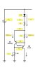
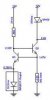
I think the WS2811 has this as the output.
Current is monitored by watching the voltage across R1.
Current is set by Vref and R1.
If what I drew is right then the WS2811 does not care if the LED is 1.5V or 3V or 9V the current will be the same. (as long as there is some headroom)
The output voltage can not be less than Vref (at 18.5mA)
I think the WS2811 has this as the output.
Current is monitored by watching the voltage across R1.
Current is set by Vref and R1.
If what I drew is right then the WS2811 does not care if the LED is 1.5V or 3V or 9V the current will be the same. (as long as there is some headroom)
The output voltage can not be less than Vref (at 18.5mA) View attachment 98658
True. However you are driving a 300ma led in this case. So you need to boost the current and keep it constant at the same time from 18.5ma! The challenge in this case is to have some headroom between Vf vs. supply voltage while considering voltage drop of WS plus two stages of Vbe on top of that. In case of Blue and Green with 9.6v for Vf, that headroom is tight. The fact that I could get a flat current starting close to 11v and going up was the key accomplishment here. For Red with Vf of 6v, you have plenty of headroom.
Looking back at pnp transistors and simulation of several iterations, they do not do a good job in capping the current on top and could become a runaway current and voltage. This happened because WS controlled a small percentage of sinking current without any regulation on the remaining sink current to ground. With the last design all 3 legs of the device are boxed in forcing led (the fourth leg) to remain at about 300ma.
This site uses cookies to help personalise content, tailor your experience and to keep you logged in if you register.
By continuing to use this site, you are consenting to our use of cookies.