Continue to Site

Welcome to our site!

Electro Tech is an online community (with over 170,000 members) who enjoy talking about and building electronic circuits, projects and gadgets. To participate you need to register. Registration is free. Click here to register now.

  • Welcome to our site! Electro Tech is an online community (with over 170,000 members) who enjoy talking about and building electronic circuits, projects and gadgets. To participate you need to register. Registration is free. Click here to register now.

Solid State Tesla Coil Burning Mosfets

Status
Not open for further replies.
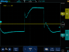
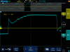
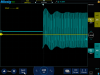
I had some MCP1407 failures driving quad IRFP3206 units at around 1500Hz. It was a combination approach of diode clamping the output to both power rails as well as introducing ferrite beads at the MCP1407 outputs to separate them and avoid shoot thru PLUS sticking a couple low ESR SMT caps in the GATE feeds to the MOSFETs to prevent a FET short from taking the driver with it. Also remember your 5 ohm GATE resistors to quell ringing.
Also I had to add a 100uF storage cap (lo ESR) near the driver to keep the Vcc rail from dipping at the driver +ve terminal. This is in Addition to a 10nF and a 100nF.

Now the drivers don't get past 35°C.
 
Ok, here are my comments. When you create your responses I ask that you please answer my questions/concerns one-by-one in an itemized list with matching numbers. This makes sure that nothing gets left out.

1) My first concern is that you're trying to drive opposite legs of the GDT with two outputs that are in-phase with each other. U5 and U6 are the same device, they're being fed the same input signal (from your feedback circuit), and their outputs are tied across two sides of the transformer primary. They're going to be fighting each other, and it's amazing that it's even working at all right now. One of them needs to be inverted (look at the UCC27321 inverting model to complement the UCC27322 non-inverting model). Was thinking you had this already. Did you change it? Is the schematic wrong, and you ARE using a '321 and a '322?

2) Second concern is the DC blocking capacitor(s) C5 and C6. What is C6? It's labeled "000".... 1uF is probably fine for C5, but I'm going to ask you to probe the GDT primary winding with your oscilloscope. If it's ringing due to the capacitance and the inductance of the GDT primary (which I suspect it is) you will need a damping resistor sized to damp the oscillations. This resistor will go in parallel with the capacitor, but you will need a smaller value capacitor (0.01uF, perhaps) in series with it to avoid creating a DC path. If you need a drawing to understand then let me know.

3) Make sure you have ~10uF ceramic capacitors located directly on the supply pins of the MOSFET driver chips. Each chip needs its own capacitor. These capacitors act as reservoirs and ensure that you can supply enough current to drive the MOSFET gates at the high frequency. I see you have 100uF on one of them, but that looks like a polarized capacitor (probably an electrolytic) whose ESR/ESL is much too high to supply the current to the MOSFET gates quickly. I'm not saying remove it, but I'm saying you definitely need ~10uF capacitors directly on the driver supply pins (as close as possible to them).

4) What is your GDT ratio? What are your transistor specs? (You may have mentioned this already but I need to know the current state of things - I know you bounced back and forth between IGBTs and MOSFETs for a bit). It is very important that the drive voltage is high enough to "slam" your transistors into saturation, otherwise your switching times will be off and you will likely draw excessive current from your driver chips (causing them to heat up).

5) How many channels does your oscilloscope have? Last I knew you weren't using a real one. It's cases like this where it would be really nice to have a real four channel scope. I need to see the switching waveforms G-S of each transistor so that I can see the timing relationships. Having all four waveforms on a single screen would be immensely helpful, or at the very least two complementary waveforms (two high-side transistors, then the two low-side transistors, perhaps).

6) The input capacitance on your LM7805 should be closer to 0.33uF and your output capacitance should be closer to 0.1uF, according to the 7805 datasheet. Not a huge concern and probably isn't causing any trouble, but best be on the safe side. It may prevent unwanted oscillations from the regulator.

7) Your 74HC14 should have a 0.1uF decoupling capacitor across its supply pins.

8) Since your feedback is fed directly from the current transformer I highly recommend placing a current-limiting resistor just before the input to the first 74HC14 gate. Otherwise you risk damaging your IC.

9) What happened to your primary coil circuit? It is not in this schematic. Do you still have a DC-blocking capacitor in series with it?

10) This is just me being picky and really has no bearing on the circuit, but the symbol for D10 shows it as a Zener but it is a Schottky. Just so you know....

Take as much time as you need to put together answers for these comments/questions. If you change the circuit, please make sure to provide an updated schematic next time you post. It is very important to keep it up to date.
 
Regarding item 1. those caps , C5 & C6 are probably introducing enough phase shift to pulse drive the FETs.
Also, are the secondaries all 1:1 ratios to maintain enough gate voltage?
I'd cut the 10Ω gate resistors to 5Ω if you want to speed switching and the drivers can handle the current.

Are the TVS snubbers heating up? I used the same series on my system(albeit 49V units with 60VDs FETs) and I was popping them real easy . Had to rig a custom snubber with a high current pulse diode into lo ESR cap in parallel with an incandescent lamp to 'burn' off the kickback.
Mosaic, I'm sure you're correct about C5 & C6, and that's probably why the coil is working at all. But that is not how it is intended to operate, so definitely something needs to be fixed. That's probably the main cause for the drivers heating up as well. 99% of the time the outputs are still fighting each other.

I also already mentioned the GDT ratios.

Regarding the gate resistance, it has to be selected carefully in order to ensure clean switching. They are there to damp the ringing caused by the GDT secondary inductance and the transistor gate capacitance. It's not a good idea to simply throw a resistor of whatever value in there without selecting the value based on the amount of ringing present on the gates.
 
Okay I will still respond with a detailed numbered response. but just to hop on this. C6 is just a 000 resistor jumper not a cap, I was editing fast when etching my board. Next was ur #1 question that was a typo, I am using one inverting and one non inverting gate driver. UCC23722 and UCC23721. I will fix these upon my response to your numbered questions, I will get u all these answers tonight by 8pm-ish GMT

Thanks guys
Don't rush. Take as much time as you need to get all the details together. I don't care if it takes a day, a week, a month, or longer. We'll get through it one way or another.
 
DerStorm8

1) Yes, Typo. Running a 321 and 322.

2) C6 is a jumper, I quickly threw that in when etching. Fixed this in new schematic bellow

3) Great Idea! Didnt think of the speed of charging. I will add caps there.

4)GDT ratio is 8-13, Gate voltage reads about 18.5v-19.75v. IGBTs are FGA60N65. Vges +-20v

5) My new scope Is a 2 channel but it is portable still. I know you can fry your bench-top scope by clamping your probe or probe gnd to something wrong. I don't have to worry about that on this one.

6) Definitely good practice, on final etched board I will correct this.

7) Would C6 in my new schematic be what your talking about here?

8)I have tried doing this, adding a resistor, when designing this circuit and was having issues with this resistor value changing my phase shift. I had great difficulties firing this TC up when a resistor was there.

9) Fixed this, Yes still the 4.7uf 600v film

10) Fair enough lol, But yes this was the program not me, I use Target3001 for some reason a MBR360 symbol shows as zener lol weird.
 

Attachments

  • SSTC5_Schem.pdf
    118.8 KB · Views: 109
The three attached photos are of my GDT Primary signal loaded. Its not ringing but there is a weird swing. These weird swings do not show on the GDT output. also on the zoomed out photo I am not sure why it waves like that. the GDT output I think has that wave as well. Not sure if thats just interference from coil running. lol hard to scope near a TC!
 

Attachments

  • 20171024200733.png
    20171024200733.png
    53.7 KB · Views: 90
  • 20171024200749.png
    20171024200749.png
    56.8 KB · Views: 99
  • 20171024200802.png
    20171024200802.png
    67.2 KB · Views: 103
Crap missed one thing. not sure how to draw it on a schematic but both gate wires from driver to GDT wrap around a ferrite bead. I attached a pic, It is the two green wires in the back running from driver board to H-bridge.
 

Attachments

  • orca-image-1508985728270.jpg_1508985729660[1].jpeg
    orca-image-1508985728270.jpg_1508985729660[1].jpeg
    392.7 KB · Views: 85
I'm at work but quick comment regarding the GDT waveforms - Ignore the initial spike and look at the rest of the waveform. It should not curve up slowly like that, it should be much more square. The slow curve indicates too high of a damping resistance. Too high of a damping resistance leads to significant switching losses, which means excessive heating. Decrease to a smaller resistance and see how the waveform looks then. Also see how it affects the temperature of your drivers.

I will try to go back to the list when I get home today.
 
I think you are referring to the gate 10 ohm resistors? But yes I have 4.5ohm I can swap too. I will change and re-post that waveform.
 
Ok, clearly the switching drive is overdamped. The inductance of the transformer coil would be slowing the required switching transition. After all it is the tuned inductance & capacitance loading in a square wave driven CLASS E amp that smooths out the switched edge harmonics.
If dropping the gate resistor values don't do the job, I'd consider direct driving the gates with the drive chips and use low ESR 10nf and 100nF paralleled capacitors in the drive lines for DC isolation.
Note the square FET switched wave form with a good gate drive below....the Batt pole 'Load' voltage image (#2) shows the effects of about 3uH of cabling on the voltage...causing a ramp compared the the 50nS rise time of the square wave from the FET Drains. The blue trace is the CT transformer monitoring the load's current flow....so u can see how that tracks with the actual voltage rise time at the load. All due to just 3uH of inductance.
Zoom-PCB-noshort-toroid.png
Batt-pole-noshort-zoom.png
 
Okay so is there any options other then direct drive? I'm a bit nervous doing direct drive with my skill level, scared of frying my driver board.

Would dropping my gdt windings lower this inductance enough? Maybe trying 5-8? Also I am probing my gdt primary at my driver board screw terminals. So prior to my ferrite bead. not sure if I need to test right on the gdt primary or if after or before the ferrite bead may change my reading.
 
Or possibly changing wire thickness that runs from driver board to h-bridge. Increase trace thickness of driver output traces(beef up with solder for now) increase on finnal etch
 
Yes, dropping the overall turns would speed things up some concerning the edge of the pulse.
Rather than changing the driver wire thickness, use double or quadruple point to point twisted driver wiring as inductance works like resistance, it drops with paralleled inductance.

Also solder thicken the gate drive traces and widen them if possible. I use desoldering braid to boost trace conduction for higher pulse currents.
 
Last edited:
Okay, well just for ***** and gigs I took my driver board out added some solder to the traces. bare with my on the horrible looking solder job I have removed and replaced stuff like 15 times lol. No clue if that'll help but wont hurt. Also found I already did add a 10uf ceramic cap right next to each driver chip. And I my toroid for GDT is 8500u, I think thats high enough.

Mosaic- Do you mean to double up or increase size on wires from my driver board to H-bridge? Im not doing point to point. look at pics, that's my setup, So beef up my green wires?
orca-image-1509059199669.jpg_1509059200129[1].jpeg
orca-image-1509059220448.jpg_1509059220818[1].jpeg
orca-image-1509059236617.jpg_1509059236980[1].jpeg

<MOD EDIT: Please watch your language!>
Nissan<Sorry>
 
Last edited:
U have a 0.1uf, 1 uf and a 100uF low ESR capacitor near to each driver chip as well to cover the gamut of transient response and reservoir stacking? That alone might do the trick IF the sag on the scope square trace is at the output pin of the Driver chip.
If the sag is at the output of the the GDT (not the input) then it's inductance can be the issue.
If the sag is ONLY at the Gates themselves then the area of concern is the connection from the GDT to the gates.
 
Status
Not open for further replies.

Latest threads

Back
Top