Electro Tech is an online community (with over 170,000 members) who enjoy talking about and building electronic circuits, projects and gadgets. To participate you need to register. Registration is free. Click here to register now.
Welcome to our site! Electro Tech is an online community (with over 170,000 members) who enjoy talking about and building electronic circuits, projects and gadgets. To participate you need to register. Registration is free. Click here to register now.
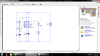
hey guys,i was working on my traffic light project and i created circuit using 555 timer(mono-stable mode) and ic 4017 but when i run the simulation in circuit wizard only first led's light up .i don't know why is this happening please help...
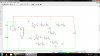
The obvious problem I see is that you do not have a resistor going from pin 7 to V+ on the 555 timer. Your current setup will probably not even provide a clock signal to the 4017. Also, is the thick green line (ground) connecting directly to Pin 3? You do NOT want this. Pin 3 should only connect to the 4017 clock input, and nothing else.
Let me know if fixing these errors helps.
Regards,
Matt
Judging by your other values shown on the circuit, and depending on how fast you want it to cycle through, you could probably place another 100k resistor between pin 7 and V+. That should give you a clock period of about 2 seconds. You can reduce the resistor value to increase the frequency, thus speeding up the cycles.
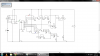
Could we see an image of the circuit while it is not being simulated? I would like to see the rest of the connections without having the colored line overlays--they are quite distracting
Judging by your other values shown on the circuit, and depending on how fast you want it to cycle through, you could probably place another 100k resistor between pin 7 and V+. That should give you a clock period of about 2 seconds. You can reduce the resistor value to increase the frequency, thus speeding up the cycles.
Could we see an image of the circuit while it is not being simulated? I would like to see the rest of the connections without having the colored line overlays--they are quite distracting
yes Sir i will upload an better image...with the logic table given in question...and introducing the resistor blows up the 555 timer it says power dissipiation is much greater 7.2w...
yes Sir i will upload an better image...with the logic table given in question...and introducing the resistor blows up the 555 timer it says power dissipiation is much greater 7.2w...
Well no wonder it's saying it's blowing it up. You did not follow my instructions!
Read carefully:
Disconnect R1 from pin 3 (the output). As I told you before, this connection should not be there. The ONLY thing Pin 3 of the 555 timer should be connected to is the clock input of the 4017. Eliminate R4. The way you connected it is not how I told you to connect it earlier. Connect the following:
Connect R1 between pin 6 and pin 7.
Connect a 100k resistor between pin 7 and V+ (12 volt supply). Alternately, since pin 4 and pin 8 of the 555 are connected to V+, you can just connect the resistor to one of them instead of to V+. It is all the same node
That's all you need to do. Try that and see what happens.
sir i decided to start all over again and doing it in small sub-circuits. starting with the 555 timer producing a pulse every 1 sec...can you please help me with that i tried it but there seems to be some problem...thnx
LTspice sees no problem with the 555 configuration in post #1. Apart from the pin 7 connection the configuration is a well-known one for generating pulses with a ~50% mark/space ratio. Since pin 7 is an open-collector pull-down output can't it validly be connected to pin3 as originally shown?
I've no idea how CW gets a 7.2W figure for power dissipation. That's at odds with the LTspice sim.
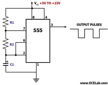
This is one of the most common astable multivibrator circuits out there for the 555:
Build the above circuit with R1 and R2 being 100k, and C1 being 10uF. Then connect pin 3 to the clock input of the 4017, with your original LED layout.
This is one of the most common astable multivibrator circuits out there for the 555:
Build the above circuit with R1 and R2 being 100k, and C1 being 10uF. Then connect pin 3 to the clock input of the 4017, with your original LED layout.
LTspice sees no problem with the 555 configuration in post #1. Apart from the pin 7 connection the configuration is a well-known one for generating pulses with a ~50% mark/space ratio. Since pin 7 is an open-collector pull-down output can't it validly be connected to pin3 as originally shown?
I've no idea how CW gets a 7.2W figure for power dissipation. That's at odds with the LTspice sim.
The datasheet for a 555 says that it must have supply bypass capacitors from pin 4 to pin 1 that are 0.1uF parallel with a 1uF electrolytic.
Then if it is soldered (not using a solderless breadboard) its frequency will be stable.
NONE of the circuits of the 555 shown on datasheets shows pin 3 connected to pin 7. Why don't you try a circuit that they recommend??
You really only need bypass capacitors if you need an extremely precise output. They are entirely unnecessary for the type of circuit the OP is creating.
The 555 causes 400mA supply current spikes caused by shoot-through on its totem pole output stage. If the supply is a weak little battery then its voltage will collapse each time the output changes state without having the important supply bypass capacitors.
Then the frequency will not be stable.
I don't deny that using bypass capacitors would be best, but for all practical purposes for this particular circuit, I don't think the OP will notice much of a difference.
On the other hand, adding 2 capacitors isn't hard, so I guess it's up to him.
I don't deny that using bypass capacitors would be best, but for all practical purposes for this particular circuit, I don't think the OP will notice much of a difference.
On the other hand, adding 2 capacitors isn't hard, so I guess it's up to him.
This site uses cookies to help personalise content, tailor your experience and to keep you logged in if you register.
By continuing to use this site, you are consenting to our use of cookies.