Continue to Site

Welcome to our site!

Electro Tech is an online community (with over 170,000 members) who enjoy talking about and building electronic circuits, projects and gadgets. To participate you need to register. Registration is free. Click here to register now.

  • Welcome to our site! Electro Tech is an online community (with over 170,000 members) who enjoy talking about and building electronic circuits, projects and gadgets. To participate you need to register. Registration is free. Click here to register now.

output error voltage and drop-out voltage in LDO

Status
Not open for further replies.

hanhan

Member
Hi.
I get stuck while reading lecture about LDO.
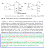
Please help me with questions in the picture below.
Here is the like to the entire lecture:
https://sites.ieee.org/scv-sscs/files/2010/02/LDO-IEEE_SSCS_Chapter.pdf

?temp_hash=e2d13eb0988f818a71b4e2af7ca3c728
 

Attachments

  • Line regulator.png
    Line regulator.png
    390.3 KB · Views: 793
Q1 - I don't have a clue. Normally we use Rout or load regulation include voltage "drop" as load current change.

Q2 - I don't understand your problem here ? For the linear regulator Vdrop is always equal to Vin - Vout.
But for NMOS reg Vdrop cannot be smaller than Vgs plus op amp positive saturation voltage. Why?
Because in this type of a regulator, series pass transistor work as a voltage follower (common drain amplifier).
And this is why Vdrop is always larger then Vgs.

3.PNG


But we can fix this issue if we replace NMOS with a PMOS which now will work as a common source amplifier.
And know Vdrop_min = Iload * RdsOn if Vin is low enough.

Also notice that this linear regulator is is nothing more than non inverting amplifier + additional transistor added to increase the op amp output current capability. Where Vin = Vref.
 
Last edited:
Thank you, Jony.

I have been reading a lot about using NMOS and PMOS in LDO. However, I am still
confused about the dropout voltage calculation in each case.

As you said, Vdrop is always equal to Vin - Vout. In LDO, it is the voltage between Drain and Source, Vds.
I also read that in LDO, NMOS acts as a voltage follower and PMOS acts as a common source amplifier. Therefore, PMOS give a lower dropout voltage compared to NMOS.

That is what I can't understand.
In your picture, it is a common source topology. I have some questions.

1. In your example, the gate G is connected to Vin. However, in LDO, it is connected with the output of error amplifier. That makes the calculation more difficult. If G is connected with the output of error amplifier, how would you calculate the dropout voltage, Vdrop = Vds, there?

2. I hope you could help me understand this part from the book CMOS High Efficiency On-chip Power Management by John Hu • Mohammed Ismai.

More: https://books.google.com.vn/books?i...6AEwBg#v=onepage&q=common-source PMOS&f=false

?temp_hash=8eb578459852c777ce9c622593dd4592
 

Attachments

  • LDO topology.png
    LDO topology.png
    243.6 KB · Views: 605
Hi,

I have a few comments.

First, a PMOS is driven from the ground up, such that the closer the gate is to ground the more it conducts. That means as long as there is input voltage there is always enough gate voltage available. But for NMOS there is not always enough gate drive available because the gate has to be higher than the source, and if the source is already very close to the drain (the drain gets the input voltage level applied to it, which is the maximum available voltage in the system) this means the gate voltage will always be lower than the level needed to drive the NMOS source very very close to the input voltage level (that's LDO operation).

Second, this looks like one of the best articles i've seen in a while. I hope i get to read more of it soon. But one small detail i noticed right away is the statement that the LDO is less efficient than a switching regulator. This statement is often true, but it's NOT always true. When the input voltage level of the LDO is close to the output voltage level we see very high efficiency, and that can easily beat a buck with a 80 percent efficiency spec. So it really depends on the actual application and the type of switchers that are actually available to use in the application at the time. It's not always as simple as input and output voltage levels though, sometimes we have to look at the average efficiency over the battery life (batter operated equipment of course) which means looking at the average efficiencies as the battery voltage falls for both types of regulator and then comparing.
 
I have been reading a lot about using NMOS and PMOS in LDO. However, I am still
confused about the dropout voltage calculation in each case.
I see your problem now, you simply forgot how NMOS voltage follower work.
As a reminder can you tell me what is the output voltage (Vout) in these three simple circuits? You can assume Vgs = 3V

10.PNG


In your picture, it is a common source topology.
Are you sure about that ?

1. In your example, the gate G is connected to Vin. However, in LDO, it is connected with the output of error amplifier. That makes the calculation more difficult. If G is connected with the output of error amplifier, how would you calculate the dropout voltage, Vdrop = Vds, there?
This error amplifier is nothing more than the ordinary op amp. And every op amp has his on output voltage range. And for the typical op amp the maximum positive voltage output voltage is 1V smaller then Vcc.
https://e2e.ti.com/blogs_/archives/...input-and-output-clearing-some-confusion.aspx
So for example for Vcc = 15V op amp can give max 14V at his output, and if we assume Vgs = 4V. We have Vout_max = 15V - 1V - 4V = 10V.
And Vdrop = Vd - Vs = 1.5V + 4V = 5V

12.PNG

Do you understand this now ?
 
Thank you, Mr Al and Jony.

@Mr Al.
First, a PMOS is driven from the ground up, such that the closer the gate is to ground the more it conducts.
Yes, I know that. The current through PMOS increased significantly as the voltage Vsg increases a little.
That means as long as there is input voltage there is always enough gate voltage available.
Vin = Vs
Vsg = Vin - Vg
Vsg will be always positive provided that Vin is larger than Vg.
Did you mean that the voltage Vg is always smaller than Vin?
Vg is the output voltage of error amplifier.
I assume that in this case the DC voltage sources for the error amplifier is also VDD. In that case as Jony said, Vout = Vg, at best, is VDD. Generally Vg will be smaller than VDD.
And it makes sense as you said, provided there is Vin, Vsg will be always larger than zero and the transistor never turns off.

But for NMOS there is not always enough gate drive available because the gate has to be higher than the source, and if the source is already very close to the drain (the drain gets the input voltage level applied to it, which is the maximum available voltage in the system) this means the gate voltage will always be lower than the level needed to drive the NMOS source very very close to the input voltage level (that's LDO operation).

Could you give an example in which the gate voltage is not enough?
Here is what I can imagine.

Input voltage: Vin = Vd: 2.3 - 2.9V
Output volage: Vout = Vs = 2V
Assuming that the error amplifier also uses Vin as DC voltage sources for biasing.
At the time Vin = 2.3V and Vout = 2V => Vdrop = Vds = 0.3V.
The maximum output voltage of error amplifier (best case) is Vin - 1 = 1.3V.
And therefore, Vgs < 0 and the transistor is off.
However, is there a perfect error amplifier that will give output voltage equal to DC voltage?
For example, if VDC = 2V then the output voltage of error amplifier will be 2V.


Jony:
I see your problem now, you simply forgot how NMOS voltage follower work.
As a reminder can you tell me what is the output voltage (Vout) in these three simple circuits? You can assume Vgs = 3V

My problem is that I usually can't accept that Vgs is almost constant as in the case of emitter follower.
If we consider Vgs is constant.

a) Vout = 5 -3 = 2V
b) Vout = 10 -3 = 7V
c) Vout = 23 -3 = 20V

Are you sure about that ?
I thought it is PMOS in your picture.
If it is NMOS then it is common drain.
In that picture, how can you know that Vds(min) = 3.5V?

Do you understand this now ?

I am still confused about the statement saying that Vdrop in NMOS is higher than that in PMOS. It seems to me that we use PMOS instead of NMOS for the reason mentioned by Mr Al not because Vdrop of NMOS is higher than PMOS.

P.S. In case of PMOS, why don't we use an error amplifier which is Vout very large?
For example, with the circuit Vin: 2.3 -3V, we use an error amplifier that give maximum output voltage about 4V.
 
Last edited:
Hello again anhnha,

When i said there is always enough gate voltage i meant the differential gate voltage, not the gate voltage measured from gate to ground. Another way of looking at this is the absolute value of the gate voltage.
But it's ok if you want to look at it as the actual gate voltage measured from gate to ground, then the explanation is slightly different.

Looking at the gate voltage from gate to ground, if the PMOS is not turned on enough all we have to do is 'lower' the gate voltage. That turns it on harder. So if we have 10v input (source) and we want nearly 10v output (drain) then all we have to do is pull the gate close to ground (assuming the right PMOS part number) and we get nearly 5v output.

With the NMOS we can not do this unless we have a gate voltage that is higher than the input voltage. For the same example using the NMOS as source follower, if we want 10v output (source) with a 10v input (drain) then we need a gate voltage that is maybe 20 volts. But we dont have 20 volts in the system, we only have 10 volts, so it's not possible to do it that way.
Another choice is to use the NMOS with source connected to ground and drain as the on/off terminal. In this case we try to get the drain as close as possibly to ground instead of +Vcc (the 10v input). This means that again we get a low voltage drop across the device, but now we are using it differently and we are not switching the 10v supply anymore we are switching ground. It's easy to get that to turn on hard because we have +10v available for the NMOS gate.

In short, the NMOS requires a gate voltage maybe 10v higher than the source. If we only have 10v available then we can not switch the 10v source on and off with it, although we can switch ground.
The PMOS is just the opposite, we can switch the +10v source but we cant switch ground.

All this changes however if we use a gate driver that can boost the voltage up to 20 volts. That means we get enough voltage then, but that requires a special driver chip.
 
Thank you, Mr Al.
I got it.
In the case of NMOS, then we need to voltage at the output of error amplifier as low as possible.
(although, it is not a must)
What is the gain requirement for the amplifier?
It is to amplify. However, we don't need a high output voltage. I can't figure out how to set requirement/specifications for the amplifier.
 
Hi,

What amplifier?
 
Hi,

Are you talking about the two circuits in post #3 ?
 
Hi,
Are you talking about the two circuits in post #3 ?
I am talking about the one on the left. It is LDO.
What is the requirement for the error amplifier? It is good with low gain, right? However, how much gain does it need? For example, if I choose the error amplifier with voltage gain = 1, is this OK?
 
Hi again,

The total gain for that circuit is made of the op amp and the PMOS. The voltage gain of the op amp is usually high and varies, but if it's a fixed value then you calculate the approximate gain of the op amp plus PMOS by noting that the transconductance leads to a current output but then the resistive load makes that a voltage value. Knowing the gm and the output circuit resistance you can then calculate the voltage gain of the PMOS stage and multiply that by the gain of the op amp.

Now knowing the gain, we would then proceed to calculate the output voltage Vout knowing the reference voltage, doing the full loop not open loop. This gives us a fixed value for the output voltage Vout which we can then compare to Vref. This then gives us a way to measure the quality of the circuit to regulate the output voltage to within some percentage from ideal.

As a simple example, say we have a reference voltage of 1.0 volt. Then after we calculate the gain of the PMOS stage and combine it with the op amp gain and then calculate the full loop so we get the output voltage result say we see 0.9 volts. This result is rather poor being 10 percent off, so we know we dont have enough gain in the op amp and/or PMOS section. If we got 0.95 volts it still isnt that good. If we got 0.99 volts then it's much better now. However, to get 0.95 instead of 0.90 meant we had to put in more gain, and getting 0.99v rather than 0.95 meant we had to add even more gain yet.

See if you can come up with the calculation for the output voltage knowing the voltage gain of the PMOS section and the gain of the op amp and i think you will see how this works. If you dont know the voltage gain of the PMOS then just substitute Apmos for now or some numerical value if you prefer.

A couple things to note:
1. The PMOS adds a lot of voltage gain to the loop which helps the steady state error.
2. With a voltage follower circuit if the gain is infinite the output voltage matches the input exactly (or some ratio exactly set by the resistors).
 
Thank you, Mr Al.
The total gain for that circuit is made of the op amp and the PMOS.
OK, I see.
The voltage gain of the op amp is usually high and varies, but if it's a fixed value then you calculate the approximate gain of the op amp plus PMOS by noting that the transconductance leads to a current output but then the resistive load makes that a voltage value. Knowing the gm and the output circuit resistance you can then calculate the voltage gain of the PMOS stage and multiply that by the gain of the op amp.

Well, I think I was wrong. My opinion was that because we use the operational amplifier with negative feedback and so, Vfb (please see the picture on the left of post #3) is ALWAYS equal to reference voltage, VBG, NO MATTER how large the gain of OAMP and PMOS are.
Is that wrong?

Now knowing the gain, we would then proceed to calculate the output voltage Vout knowing the reference voltage, doing the full loop not open loop. This gives us a fixed value for the output voltage Vout which we can then compare to Vref. This then gives us a way to measure the quality of the circuit to regulate the output voltage to within some percentage from ideal.

As a simple example, say we have a reference voltage of 1.0 volt. Then after we calculate the gain of the PMOS stage and combine it with the op amp gain and then calculate the full loop so we get the output voltage result say we see 0.9 volts. This result is rather poor being 10 percent off, so we know we dont have enough gain in the op amp and/or PMOS section. If we got 0.95 volts it still isnt that good. If we got 0.99 volts then it's much better now. However, to get 0.95 instead of 0.90 meant we had to put in more gain, and getting 0.99v rather than 0.95 meant we had to add even more gain yet.

This seems to be the "trial and error" method. In your example, I think you meant Vout is the feedback voltage,Vfb. We keep changing the gain of amp and PMOS until Vfb = VBG (reference voltage).
Is there a definitive way to find the total voltage gain of amp and PMOS?

In the end we want Vfb = VBG. However, when I substitute that result in the circuit, the differential voltage of the amp (Vfb - VBG) is zero and that makes my calculation go nowhere.

A couple things to note:
1. The PMOS adds a lot of voltage gain to the loop which helps the steady state error.
2. With a voltage follower circuit if the gain is infinite the output voltage matches the input exactly (or some ratio exactly set by the resistors).
It would be great if you could explain more about this.
Also, in #2, are you talking about HDO (High DropOut Regulator)?
 
Last edited:
Hi again,

Well it is only trial and error for that explanation, once you do the math you can solve for the desired gain. Let's take it from the top :)

Starting with the equation for Vout knowing the open loop gain of the op amp A1 and the voltage gain of the PMOS A2, we have the simple:
Vout=(Vfb-Vbg)*A1*A2

If you take a minute to think about this, you'll see that the output really depends on the difference between the two voltages Vfb and Vbg. Since this difference must be small so that we can get an output voltage that is reasonably close to Vbg, that means that the output really depends on a tiny difference between the two. It's that tiny difference that makes this thing work at all, and that is kind of amazing.

Now since Vfb is dependent on the output voltage Vout, and the gain of R1 and R2 can be summarized as just another gain A3, we can substitute this into the equation and we get:
Vout=(Vout*A3-Vbg)*A1*A2

Now we solve for Vout explicitly and get:
Vout=(Vbg*A1*A2)/(A1*A2*A3-1)

That's our whole loop feedback equation and we can see that Vout depends on Vbg (the reference voltage) and the three gains. We can also lump A1 and A2 into A12=A1*A2 and get:
Vout=(Vbg*A12)/(A12*A3-1)

We can also make A3=1 for the case where Vfb is tied directly to Vout, or rather the voltage division of R1 and R2 cause Vfb to be very nearly equal to Vout:
Vout=(Vbg*A12)/(A12-1)

Now if we did a few numerical calculations with this result we'd find that the output is slightly higher than the input because of that minus term in the denominator. So for a gain A12=10 we get:
Vout=Vbg*10/9=Vbg*1.11111111
which is about 11 percent high.

With a gain of 100, we get:
Vout=Vbg*100/99=Vbg*1.01010101
which is only about 1 percent high.

Increasing the gain further results in less and less steady state error.

Of course normally we just want to ensure that the output is reasonable close to the input, but within some predetermined limit. So we simply solve for the gain A12. Starting with:
Vout=Vbg*A12/(A12-1)

we get:
A12=Vout/(Vout-Vbg) for: {Vout>Vbg}

or in terms of the error voltage itself:
A12=Vout/Verror

so if we want an error of only 0.01 volt we would do this:
A12=1.01/0.01=101

so we need a gain of 101 to get an output that is just 0.01 volt higher than Vbg. If you try a little you can turn this into a percentage equation so you can calculate the minimum gain based on a percentage error rather than an absolute voltage error.

Next we can talk about the gain of the PMOS if you like. To do that we need actual resistances for R1 and R2.
 
Last edited:
Hi, Mr Al.
Thanks a lot for the interesting explanation. I understand a lot from the difference between LDO and HDO to the role of amp and PMOS gain in reducing voltage error.
From that explanation, I see that we need A12 as large as possible. As A12 -> infinity the output is equal to Vbg.
I am eager to read your next post about the gain of the PMOS. However, I am not sure what you would say next. From above, it also should be as large as possible.
 
Hello again,

Well you are pretty much right there i am happy to say, but there is a catch with the PMOS. With the NMOS (voltage follower) the gain being very large makes the error go to zero or at least near that, and with the PMOS with purely resistive elements we might have to be more careful because we dont always have pure resistance in the load and as you already know the PMOS has capacitance and this can ruin our perfect circuit by making it unstable. That would have to be investigated later too because as you probably know gain is important in feedback amplifiers because with some gains they are stable and with other gains they may not be. In fact to be more thorough i would look at the NMOS more critically too just to make sure.

To get an understanding of the PMOS we can start with the simplified model where we have a zero gate threshold and no capacitance. The output current is then just dependent on the absolute gate voltage (gate voltage measured source to drain). The output current is then simply:
Iout=gm*Vg

so if we have a gm of 0.1 and a gate voltage of 2 volts we have Iout=0.1*2=200ma.

Now with a resistive load that is much lower than the divider resistors R1 and R2, we have Rout=Rload, but with no load we have only R1 and R2 in series so we would have Rout=R1+R2.
With either of these conditions, we then have Vout=Iout*Rout where Iout is from above.
Since Iout=gm*Vg with this simplified model we then have Vout=gm*Vg*Rout. This leads to the gain:
A2=gm*Rout (although it is actually an inverter so it would be negative)

So the total gain is A1*A2=A1*gm*Rout.

Note we have not yet considered any output capacitance, gate capacitance, or gate threshold voltage. The gate threshold voltage puts a requirement on the A1 gain because we have to have enough gain to get the op amp to be able to ramp up (or down) to whatever gate voltage that is required to start the PMOS conducting. So there is a little interplay there in the real world circuit.

Are you starting to see how this works now? We've only used a resistive load but if the load contained capacitance then we have to start looking at the circuit in terms of frequency response and maybe time domain response as the article did. That is how we could investigate stability.
 
Hi, Mr Al.

To get an understanding of the PMOS we can start with the simplified model where we have a zero gate threshold and no capacitance. The output current is then just dependent on the absolute gate voltage (gate voltage measured source to drain). The output current is then simply:
Iout=gm*Vg

so if we have a gm of 0.1 and a gate voltage of 2 volts we have Iout=0.1*2=200ma.

Now with a resistive load that is much lower than the divider resistors R1 and R2, we have Rout=Rload, but with no load we have only R1 and R2 in series so we would have Rout=R1+R2.
With either of these conditions, we then have Vout=Iout*Rout where Iout is from above.
Since Iout=gm*Vg with this simplified model we then have Vout=gm*Vg*Rout. This leads to the gain:
A2=gm*Rout (although it is actually an inverter so it would be negative)

So the total gain is A1*A2=A1*gm*Rout.

I got this except for the red bold phrase. I believe you meant "gate voltage measured from drain to gate".

Note we have not yet considered any output capacitance, gate capacitance, or gate threshold voltage. The gate threshold voltage puts a requirement on the A1 gain because we have to have enough gain to get the op amp to be able to ramp up (or down) to whatever gate voltage that is required to start the PMOS conducting. So there is a little interplay there in the real world circuit.

In this case, it seems that you are talking about LDO with PMOS as a pass element. Should it be the upper limit voltage for A1?
If A1 is too large then Vsg = Vs - Vg = Vin - Vg will be go below threshold and PMOS stops conducting.

Are you starting to see how this works now?

I still have some problems.

We've only used a resistive load but if the load contained capacitance then we have to start looking at the circuit in terms of frequency response and maybe time domain response as the article did. That is how we could investigate stability.

I got it generally. However, I need to do it to get more insight.

Well you are pretty much right there i am happy to say, but there is a catch with the PMOS. With the NMOS (voltage follower) the gain being very large makes the error go to zero or at least near that, and with the PMOS with purely resistive elements we might have to be more careful because we don't always have pure resistance in the load and as you already know the PMOS has capacitance and this can ruin our perfect circuit by making it unstable. That would have to be investigated later too because as you probably know gain is important in feedback amplifiers because with some gains they are stable and with other gains they may not be. In fact to be more thorough i would look at the NMOS more critically too just to make sure.

This what I am confused. Could you explain why PMOS has capacitance while NMOS is not? I thought that they have the same parasitic capacitances.
 
Hi,

You need to look at the basic setup first before considering the capacitance.

When i said gate voltage i meant gate to source, not gate to drain. The gate voltage is measured from gate to source not gate to drain. That's true of any MOSFET.

The gain problem comes in when capacitance is added to the circuit but i think we should wait on that.

It's not the upper limit for the reason of just turning on the MOSFET. The upper and/or lower limit of the gain comes in later when the dynamic characteristics are examined. For now, just look at the PMOS has having zero threshold voltage and no capacitance. See if you can calculate and understand what is happening.

Note that with zero output when we apply Vbg the difference is large so the output of the op amp goes lower, thus turning the PMOS on harder, thus raising the output voltage, thus raising Vfb, thus making the difference lower, thus making the op amp output go a little higher to drive the PMOS a little less. Eventually it reaches a point where everything balances out. When the circuit balances out we have Vout=Vdiff*TotalForwardGain, where the TotalForwardGain is equal to A1*A2 and Vdiff is the absolute difference between Vbg and Vfb. So for a difference of 0.01 volts and a gain of 101 we get as output 1.01 volts, and with Vbg=1.00 volts Vdff then equals 0.01, so it works out.
When we start to consider the capacitance that delays everything so it does not balance out as simply. But look at it like the above first and see what you think.
 
Hi.
When i said gate voltage i meant gate to source, not gate to drain. The gate voltage is measured from gate to source not gate to drain. That's true of any MOSFET.
Yes, it was my mistake. I did mean "source" not "drain".
Note that with zero output when we apply Vbg the difference is large so the output of the op amp goes lower
I am not sure this. You said that the output voltage goes lower. Do you mean that it is lower than the one as the PMOS is completely OFF?
Initially, Vout = 0V. Therefore, Vfb is also 0V, Vdiff =Vbg. At the output of the amp, Vg (measured from gate to ground) = Vdiff * A1.
I think Vdiff * A1 should be always smaller than source voltage (or Vin) otherwise PMOS will never turn ON and the circuit is not able to start.
If Vdiff*A1 is smaller than Vin, PMOS will be ON and the output voltage Vout increases. This results in Vfb decreases and Vdiff decreases => PMOS turn ON more and Vout increases more as you said.

In the case A1 is too large, initially Vdiff is too large and exceeds Vin, therefore PMOS keeps being OFF.
This is the upper limit A1 that I meant.
Is this wrong?
 
Status
Not open for further replies.

Latest threads

Back
Top