Electro Tech is an online community (with over 170,000 members) who enjoy talking about and building electronic circuits, projects and gadgets. To participate you need to register. Registration is free. Click here to register now.
Welcome to our site! Electro Tech is an online community (with over 170,000 members) who enjoy talking about and building electronic circuits, projects and gadgets. To participate you need to register. Registration is free. Click here to register now.
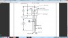
I want to ask one thing more as i have uploaded the .brd but when i open(in Allegro PCB editor) it i always have to place component due to which all aligment is changed , but how to open it ass the aliment was saved before...?
simply click manufacture - artwork, check both bottom and top, click create artwork. You will get two files, BOTTOM.art and TOP.art
The board is not yet routed, so there will be a warning about drc.
---- Photoplot outline rectangle not found ... using drawing extents
Results from parameter file ...
DEVICE-TYPE GERBER_RS274X
OUTPUT-UNITS MM
FILM-SIZE 2400000 1600000
FORMAT 2.5
ABORT-ON-ERROR NO
SCALE 1
SUPPRESS-LEAD-ZEROES YES
SUPPRESS-TRAIL-ZEROES NO
SUPPRESS-EQUAL YES
UNDEF-APT-CONT NO
WARNING: Generating metric output data from an english database
may cause slight roundoff error of coordinates in output file.
I want to ask one thing more as i have uploaded the .brd but when i open(in Allegro PCB editor) it i always have to place component due to which all aligment is changed , but how to open it ass the aliment was saved before...?
usually there is some note that the dimensions are in inch(mm) so 0.025(0.63) means 0.025" and 0.63mm
Also note that 0.025"=0.63mm, who would have guessed that..
This site uses cookies to help personalise content, tailor your experience and to keep you logged in if you register.
By continuing to use this site, you are consenting to our use of cookies.