Hi All,
I am playing around with various configurations of a mosfet load switch and have stumbled across a problem i dont quite understand.
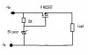
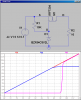
Ive attached the circuit below. Basically its a very simple P mosfet load switch. I dont understand why the mosfet does not turn on at the value of the zener. As soon as the zener conducts it should pull the gate low with respect to the source pin and the mosfet should switch hard on. However in reality it actually switches on at around 11 to 12 volts.
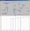
I am using an led as a simple load so its hard to see when it actually does switch on because there is no snap action, only a gradually increasing brightness until its fully on.
Any ideas what is causing this?
I am playing around with various configurations of a mosfet load switch and have stumbled across a problem i dont quite understand.
Ive attached the circuit below. Basically its a very simple P mosfet load switch. I dont understand why the mosfet does not turn on at the value of the zener. As soon as the zener conducts it should pull the gate low with respect to the source pin and the mosfet should switch hard on. However in reality it actually switches on at around 11 to 12 volts.
I am using an led as a simple load so its hard to see when it actually does switch on because there is no snap action, only a gradually increasing brightness until its fully on.
Any ideas what is causing this?