Continue to Site

Welcome to our site!

Electro Tech is an online community (with over 170,000 members) who enjoy talking about and building electronic circuits, projects and gadgets. To participate you need to register. Registration is free. Click here to register now.

  • Welcome to our site! Electro Tech is an online community (with over 170,000 members) who enjoy talking about and building electronic circuits, projects and gadgets. To participate you need to register. Registration is free. Click here to register now.

LM358 Booster for Rail to Rail Output

Status
Not open for further replies.

MrAl

Well-Known Member
Most Helpful Member
Hi there,

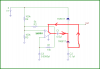
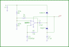
Here's a circuit that boosts the positive power supply for the LM358 (or other similar op amp) using one section of the LM358 so that the other section can be used as a rail to rail output op amp even with a power supply voltage of only 5 volts. It's a simple boot strapped voltage doubler, so even when powered by only +5v the output of the second section of the LM358 should be able to swing from 0v to +5v without the typical 1.5v voltage drop. Of course it should only be used for light loads.

This works theoretically, but i do have some fears for a practical circuit.
For one, the output of the oscillator section (shown in the schematic) might have to output the max current all the time it is running.
Second, although the output is fairly smooth, it isnt perfectly smooth but has a small sawtooth ripple.

If anyone wants to try the circuit out in real life that would be great.
 

Attachments

  • LM358_VoltageBooster-01.gif
    LM358_VoltageBooster-01.gif
    6.9 KB · Views: 1,352
Mr. Al

>I don't see how it works.
>At start up, C2 has 3.5 volts because of the two diode drops.
>When the output of the LM358 is low it charges up C1. There is one diode loss and the LM358 cannot pull to ground. Maybe there is 3 volts on C1.
>When the LM358 goes high....
>>The VCC pin gets its power from C2.
>>I don't see how the LM358 can stand on C2 and lift C1 to charge C2.
>>I think the "charging" current will flow (VCC pin, Out pin C1, diode, back to VCC pin)
>>How does C2 get pumped up?
 
I simulated the circuit, which is a simple voltage doubler, in LTspice but the output voltage was very wimpy and couldn't drive even a 100kΩ load so I added a couple of output transistors to boost the current. Now the circuit has no trouble generating 8V with a 100Ω load (R5). I increased some of the capacitor sizes for the increased output load and to reduce ripple.


5V Boost.gif
 
Hi there Ron,


In theory this is how it works...

When power is first applied, C2 should have around 4v across it. That's because the two diodes are Schottky diodes not regular Si diodes.

With 0v across C3 the output of the LM358 is high, which means it might have 3v at the output or maybe a bit less, so C1 charges up just a little bit with left side negative and right side positive. C3 starts to charge, and eventually becomes higher than the 2 x 100k voltage divider voltage (note an improvement might be to power the voltage divider from C2 rather than from +5v). The output of the LM358 ramps down low toward 0 volts. As the output gets lower, C1 charges up more with the most positive still on the right side. Meanwhile, C3 is discharging. As C3 voltage gets lower, the output of the LM358 again goes high, forcing the left side of C1 higher than before. Since before C1 left side was near 0 volts and the right side was near 4.5v, the cap voltage is around 4 volts. With the left side near 4v (the voltage across C2) and the cap voltage around 4v, the right side then goes to around 8v. This pumps up C2.

This was the quick view and in real life it should take some cycles to pump C2 up to it's maximum.

Remember this circuit has not yet been tried out in real life. It should work because C1 charges up based on the upper diode and the LM358 ground terminal, so C1 charging does not depend on the voltage present on the positive power supply pin of the LM358. Thus the energy entering the pump part of the circuit comes from C1 charging up.
Also, when C1 discharges it is partially floating so the current should divide between C2 and the positive supply pin of the LM358.

Does it really work in real life? We'd have to try it and see. If it does in fact work there may be an idea frequency to run it at as well as ideal cap values for C1 and C2. I started with the ratio 5:1 but that was just a quick guess.
 
I simulated the circuit, which is a simple voltage doubler, in LTspice but the output voltage was very wimpy and couldn't drive even a 100kΩ load so I added a couple of output transistors to boost the current. Now the circuit has no trouble generating 8V with a 100Ω load (R5). I increased some of the capacitor sizes for the increased output load and to reduce ripple.


View attachment 87416


Hi,

That's interesting too, but this is NOT intended to be used as a voltage doubler circuit. That "Vo1" in the original schematic is just a place to measure the voltage getting to the LM358, not as an actual output. The idea is to use the other half section for something that requires fairly low current. The intent was to get the output of the other section of the LM358 to be able to get all the way up to +5v without requiring a power supply voltage higher than 5v. That effectively makes the LM358 output rail to rail.

As i said that new circuit is interesting too, but hopefully we dont need the extra parts. There is a chance that we will anyway though; we'd have to do some real life testing.
My last remaining fear is that C1 acts like it is almost shorted out so the current does not split (in order to charge C2). This has to be tried to find out. It depends on how the output of the LM358 behaves when it goes high...does it becomes more of a true voltage node (relative to the caps current draw) or does it act more like just a voltage drop between the top of C2 and output? That would have to be tested.

Another idea is to use a single NPN on the output with inductor and just make the output look like a regular switching boost converter. I was hoping to avoid all that though.
 
Last edited:
I simulated the circuit, which is a simple voltage doubler, in LTspice but the output voltage was very wimpy and couldn't drive even a 100kΩ load so I added a couple of output transistors to boost the current. Now the circuit has no trouble generating 8V with a 100Ω load (R5). I increased some of the capacitor sizes for the increased output load and to reduce ripple.
Your circuit solves the problem. The transistor Q1 gets its power from the battery not C2.
You can't take power from C2 to charge C2. (original circuit)
 
That's interesting too, but this is NOT intended to be used as a voltage doubler circuit. That "Vo1" in the original schematic is just a place to measure the voltage getting to the LM358, not as an actual output. The idea is to use the other half section for something that requires fairly low current. The intent was to get the output of the other section of the LM358 to be able to get all the way up to +5v without requiring a power supply voltage higher than 5v. That effectively makes the LM358 output rail to rail.
...................
It may just boost the voltage and not "double" it but it is a voltage doubler type circuit.

I understand that Vo1 is not an output but is just to power the other op amps. Your circuit does work in my simulation with no load but even a 100kΩ load (less then the other op amps likely would draw with reasonable feedback loads) reduces Vo1 to less than 6V. That's why I added the two transitors. An actual circuit may work better than my simulation but I don't think that's likely. ;)
 
Last edited:
Hi again,

Yes, i thought there would be problems that's why i wanted to post it here.

I partially agree with Ron as to the C2 cap having to do too much work, but i think why we are seeing the circuit work ni simulation is because the output of the LM358 acts in part as a true voltage node, in that it is not just powered by C2 it is also powered by some internal LM358 capacitance to ground which would mean there are three caps in the boost part of the circuit not just two. This capacitance would be small however, so that is probably why you see a large drop in voltage with even a very light load.

So with all this in mind, yes there is a need for more modifications. I like the two transistor driver idea but i was hoping to keep it even simpler, and mainly just for driving say 5ma so the second half of the LM358 could be used for some practical purpose as a rail to rail output op amp.
 
I think the fundamental problem is that you are asking the op amp to output more current than is supplied to it, which is not possible. It's sort of a perpetual-motion bootstrap that can't work.
 
Last edited:
Hi,

What is actually taking place is C1 gets almost shorted out so C2 can not charge.
If you trace the current path for C1 you'll see that any current coming out of the op amp goes through C1 and then through the lower diode then to the plus op amp power rail then to the output which leads us right back to the cap C1.
The only reason C2 charges at all is because of the transistor drop in the output of the op amp and because there is some small op amp output capacitance to ground, which allows C2 to charge but with only a small amount of energy so even a light load hogs it down.

So we need a mod somehow, and it looks like this may require at least one transistor.
 
When the LM358 pulls down the current flows in the green direction. Charging up C1.

When the LM358 lifts up it tries to short VCC to OUT pins. Current will flow in the red circle and will not flow into C2. You just short C1 across the diode. I don't see any current in C2.
upload_2014-7-22_7-29-20.png
 

Attachments

  • upload_2014-7-22_7-23-50.png
    upload_2014-7-22_7-23-50.png
    9 KB · Views: 319
Hi Ron,

I thought that was similar to what i had said in post #10 right? Are you saying that you can not even see how a tiny current can flow into C2 and thus charge it up at least a little?

If the latter is the case then the reason you can not see this charge current is because your diagram and current flow lines are too over simplified. For example, the output does not switch immediately from a low near ground to a high near the positive supply pin of the op amp. Instead it takes some time to ramp up. During this ramp time there could also be current flow from the ground pin up to the output of the op amp and through C1 and then through C2.
However, from what we are seeing here i dont believe that will be enough to get the circuit to function as desired in it's intended use, which although it is for low current it's not that low. The time it spends in the ramp period probably isnt long enough, which suggests possibly a triangle wave would work better (havent looked at this yet though) as with an integrator. Might be a little difficult to set this circuit up though.
Possibly a sine oscillator would work better too, but havent looked at that either yet.
 
It's interesting. When I try it with my 358 model in spice it just bootstraps up to about 28 volts. If I use one of LT's models for an op amp that pulls to ground it doesn't do anything.
I think what Ron is saying is that the current to charge the cap above Vcc has to come from the cap - won't work I think.
 
Deleted duplicate.
 
Last edited:
As an alternate to transistors you could use a single CD4049 Hex Inverter chip (or a CD4050 Hex buffer) at the op amp output. Connecting the 6 in parallel boosts the voltage to about 7V with a maximum current of about 15mA in my simulation. You also should add a 1kΩ resistor in series with the op amp output to limit the overdrive current to the CMOS input when the voltage exceeds 5V.
 
BootstrappedLM358.jpg

BootstrappedLM358detail.jpg
Here is my version of a LM358 bootstrapping its own Vcc. First I created a multivibrator that runs at about 8kHz. I then connected it to a modified charge-pump voltage-doubler. This LTSpice model of the LM358 does a credible job of modeling the LM358's Vol, Voh and the max current from the output pin...

It only pumps the Vcc pin to ~8V, but that might provide the headroom Mr. Al was looking for...

I just noticed the similarity to Cruts' circuit. I was able to make it work without a buffer.
 
Last edited:
Cruts circuit is totally different. It gets power for the 5V source to lift up the supply cap.
 
Cruts circuit is totally different. It gets power for the 5V source to lift up the supply cap.
So does the one I posted. Look at the current through diode D1. It charges C2 when U1 switches low. C2 then discharges into C3 via D2 when U1 switches high.
 
It's interesting. When I try it with my 358 model in spice it just bootstraps up to about 28 volts. If I use one of LT's models for an op amp that pulls to ground it doesn't do anything.
I think what Ron is saying is that the current to charge the cap above Vcc has to come from the cap - won't work I think.


Hi,

Yes that is right overall. So now how to make it work. It could be that we must add at least one transistor.
There's another possibility if we allow the use of an LM324 rather than an LM358, because that would give us at least one more op amp section to work with. Maybe that second section could be used somehow.
This is just one of the many possibilities though, dont hold back from thinking up new ideas even if they dont work at first.
 
...I don't see any current in C2...
C2 in your circuit only carries the supply ripple current; after-all, it is just a filter capacitor between the opamp's Vcc and ground.
 
Status
Not open for further replies.

New Articles From Microcontroller Tips

Back
Top