Electro Tech is an online community (with over 170,000 members) who enjoy talking about and building electronic circuits, projects and gadgets. To participate you need to register. Registration is free. Click here to register now.
Welcome to our site! Electro Tech is an online community (with over 170,000 members) who enjoy talking about and building electronic circuits, projects and gadgets. To participate you need to register. Registration is free. Click here to register now.
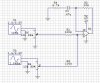
The i36-mix module is definitely unusual, but we had a few unusual things going on that we had to address. For example, all the amps are non-inverting, which is bad manners, but our hand was forced. And handling both DC and AC signals simultaneously. There's no question that there are different ways to address these things, but here's why we did what we did, opamp by opamp, moving left to right across the schematic:
U3-U5 - input buffers. These are required because system rules for our modules are that 1meg input impedance is preferred. Putting pots directly on the input would violate that system rule.
The pots. That was the simple part.
Passive AC/DC path splitting. Ok, so most audio systems have split +- rails, but we only have 0 to 5V. Also, for littleBits, every module must "work" with any other module. And Many/most of our modules operate with DC voltages ranging from 0 to 5V. So we need a DC path to comply with system rules. Then, because it's a mixer, we have to choose: do we scale both inputs at unity (so it CLIPS when both inputs are at 50%) or do we scale both inputs at 50%, so with both inputs at 100%, the output is 100%? We chose the latter.
The AC path through C1 had to be sensible for the types of inputs we were using for, which were our synth modules mainly. Those modules generaly produce large scale if not full scale signals. Basically, we tuned this by ear, and there's about 3dB of gain at signal frequencies. That's hard to see because the impedances of the passive AC/DC splitting interact. Why did we do that? It kinda seems like the weirdest part of the circuit. In this case, simply to save the cost of more opamps.
So U2 is the AC path non-inverting recovery stage. With a gain of 4 (33k/10k +1) to compensate for lasses in the passive AC/DC split, we end up around +3dB, which again, sounded best.
U4 is a non-inverting DC recovery stage, referenced to ground for DC accuracy. Importantly, this stage must be non-inverting because of the single supply and the input polarities. That means U2 must also be non-inverting.
U1 is the output driver. Again, has to be non-inverting because of U4. Required to meet system spec of low impedance output of the module.
So I know it's a bit unusual, but it solves the "we need to pass both AC and DC signals through a single supply system" problem without adding more op amps. We are under fairly substantial cost pressures for our designs, so we had to select the minimum number of opamps that complied with system rules.
I'm not on the forum continuously, but hit me with your questions and suggestions, and I'll answer as best I can.
The input path is for electronic volume control. The diode gives selectable attack and decay times. The LTP current is controlled by the charge on the shunt capacitor after the diode.
It is a pleasant surprise to have the original designer come online and explain the reasoning behind his circuit. Out of context, the circuit looks bizarre, but your explanation makes it perfectly reasonable. The one thing I would question is the lack of a low value resistor between the last op amp and the output connector.
Good point. An output resistor is good practice, so you're right to question the omission.
The reason we don't use one is because we want to save the cost of a resistor and the board space it takes up. (!) At littleBits one of our primary objectives is to drive every penny of cost out of our designs that we can. And since most of our modules are 2cm x 4cm or less, every square millimeter of real estate is precious.
We can make that decision because we have extensive field experience with our opamps, and they have very robust outputs. Over the last few years we have done tons of real world tests with our exposed electronics in difficult use conditions (like booths at MakerFaire with 100s of people handling them for hours, stress tests on the bench, ESD attacks, etc.). We also have hundreds of thousands of customer units in the field. And as it turns out we have a very low failure rate, mostly associated with the mechanicals of the designs. I can count on one hand the number of failures that I have seen that involve opamp failure of any sort.
Certainly there will be failures in the field that are not reported, but I guess my point is only that we have a lot of evidence that even though we are breaking a "rule", in this case, we are confident we can get away with it.
Geof: looking back at the diagram I see you have an ESD diode there so that is probably a help. The other reason for using an output resistor is that most ( all?) op amps become unstable if they have too much capacitive load. ( I should have looked at the LV321 data sheet first, they may be able to tolerate this.)
I also wonder about the separate AC/DC paths. It is very easy to make the gain of an amp different at AC than DC. Since this would eliminate U2 and parts and render U1 redundant, I'm curious as to why you didn't do that.( I think I see why: if the DC is close to the rail the signal might clip. With a separate path you can keep it centered.)
I feel a bit guilty taking up your valuable time and thank you for the answers you have provided.
You know what, you're totally right. Assuming it all works, we'll be removing two opamps from the next revision! Thanks!
I think this was a case of concept lockup. We were so focused on the differences between the AC and DC paths, that we overcomplicated things.
Geof: you are welcome and thank you. Your diagram shows the basic concept. I would suggest that you tie the summing junction to the half supply point as this would keep the input within CMR even if both pots are at max/min. Op-amp feedback would also be referred to V+/2, and would have both DC and AC gain.
This site uses cookies to help personalise content, tailor your experience and to keep you logged in if you register.
By continuing to use this site, you are consenting to our use of cookies.