Continue to Site

Welcome to our site!

Electro Tech is an online community (with over 170,000 members) who enjoy talking about and building electronic circuits, projects and gadgets. To participate you need to register. Registration is free. Click here to register now.

  • Welcome to our site! Electro Tech is an online community (with over 170,000 members) who enjoy talking about and building electronic circuits, projects and gadgets. To participate you need to register. Registration is free. Click here to register now.

INSIGNIA LCD HDTV help

Status
Not open for further replies.
I thought I'd update what I've found so far during my spare time since my last post:
I've tested just about every linear regulator/FET/diode on the Logic board, with nothing turning up as a failed component (yet).


I also have replaced a couple of caps which showed signs of failure during my ESR test in both the PSU and the main Logic board. Not much really came of this, though the nominal voltage across the 12v line jumped up by roughly 20mV.

I have also tested every line coming from the PSU with a known load resistance. The results with a 11Ω resistor (this time I did not lose the paper):
(I'm not sure how valid an Rth statement is here, but why not)

5V line: Vth=5.24V Δ V=-0.11V I=0.464A >> Rth=0.2360Ω
9V line: Vth=9.05V Δ V=-0.07V I=0.820A >>Rth=0.0858Ω
12V line: Vth=11.42V Δ V=-0.20V I=1.02A >>Rth=0.4444Ω
--and I kinda ingored the 24V line this time

Now, because of this data, specifically the 12V line, I thought it required a bit more investigation. Not only because of it's Rth for a high current supply (assumption made b/c it's circuitry looks a bit more complicated than just a linear regulator), but because while researching this particular supply, I have found forum posts where others have found that this particular supply's nominal and in circuit voltage is quite a bit higher (floating between 14V-16v) than what I have.

So, taking the lazy approach at first of just replacing the line, I checked out a supply from my school, cut the lines in this TV set from the 12V line, and spliced in the lines from the borrowed supply. End result:

******IT WORKED!!!*******
(backlight fired up and the screen yielded a floating NO SIGNAL image)


Only for a short period of time though. Being the Dumb*** I can be sometimes, I had walked away from it for roughly a minute while powered on, to find it had shut off. I'm not sure how much current the thing was using as the sub-supply's amp meter was peaking above what it could read, but I know it was more than an amp. Unfortunately, I have not been able to repeat this trial with the same results, but I've made some progress atleast.

For now though, along with testing the borrowed supply to make sure I don't have to replace it, I intend to begin replacing components on this PSU.

So, for anyone whom read through most of that,
any suggestions on what to look for/where to start?
I know some of these components will need to be tested out of circuit, but I'll be honest with ya here, I fear with the way some of these FETS are mounted, I'll be doing more harm than good removing them.

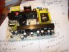
(before I forget, it's part# is 782.32HU25-200-B)
 
Last edited:
Pictures would help, wouldn't they: (my bad)
 

Attachments

  • 100_4481.JPG
    100_4481.JPG
    880.3 KB · Views: 862
  • 100_4482.JPG
    100_4482.JPG
    1.3 MB · Views: 424
Hi again!

Ahh good man, the process of elimination :)

So it looks like that 12V is dodgy, as it worked when you powered it using a seperate 12V supply. I imagine it shut off because of thermal cut-off form your bench power supply - you mentioned current was peaking above what you could read, over an amp, implying the bench supply could only kick out an amp - so perhaps another test using a high current 12V supply. I'm sure its regulation doesn't have to be great, so an ATX PSU from a PC would work, and could supply a fair amount of current on the 12V rails.

I looked at the pics, and altohugh I'm not overly experienced here, but there appears to be tthree switchmode transformers used. That thick dotted black line indicates the seperation between mains/primary side (the dangerous bit) and the low voltage side, as you can see, only two transformers, a couple of optoisolators, and a few caps cross this line. Of the two transformers, the smaller one (left middle of the board) looks like it handles low current, with only one output, the biggest transformer looks like it has 3 or 4 outputs - I am guessing your 12V is on that. The large one at the back left appears to step down mains voltage to a lower voltage, perhaps 60v? which then feeds the two switching supplies, that step this down even further.

Normally, in flyback converters, and forward converters (flyback for<100W, forards are using in ATX supplies for > 100W generally) theres multiple voltage outputs from the transformer. The swithing supply uses just one voltage for regulation, and the others track this (cross regulation). The reaons I brought that up is, for a mlutiple output transformer, if one voltage line sags (say the 12V sags because of too much load), then the other voltages form that transformer will do the same. But seeing as just the 12V line goes here, AND you've tested what its powering to make sure that isn't shorted and drawing excess current, then its most likely the circuitry between the 'big' transformer, and the 12V output.

The above is all guess work because I'm not too well at the moment, and finding it hard to concentrate, so perhaps I'll look into it in more detail later this week (that is, stare at those pics lol)

Good luck, and well done on narrowing it down!
 
I noticed the SMPS controller chips on that board are SMT. Might be worth googling the part numbers, as often manufacturers use the 'typical application schematic' as a close guide, so whilst component values will be different, it'll give you a good 'typical schematic' of what you're looking at. Heres a goodone I just found:

https://www.electro-tech-online.com/custompdfs/2011/10/NCP1605LCDTVGEVB_MANUALPDF.pdf page: 2

Has two mains inpuit filters, a PFC (power factor correction) circuit - that transformer back left -, and two seperate SMPS's. Just like yours :D

Notice the dual diodes on the outputs of the main SMPS tranformer, theres 12,24 and 30V out on that one, with the 12V out being 3A. Theres just dual diodes,caps, and a filter inductor there. My 'guess' is, if yours is similar to this, then that dual diode has gone, or its output cap has failed so it's voltage sags as it can't keep up.
 
Last edited:
Thanks man, You certainly have given me quite a bit to work off of here! Following the schematic you gave me (generally) and comparing it with the datasheets I've pulled up of a few of the other components, I can quite easily see a few components I'll need to test out of circuit (including one of those dual Schotty diodes in the Front right). For now though I really should probably return to my classwork...

I hope you feel better man. Life is hard to enjoy when some form of sickness is involved.
 
check the small electrolytics on both the primary side as well as the secondary side, some of them may be dried out, especially if they are near heat generating components. this will cause some of the supplies to be noisy, or have poor regulation. the small transformer on the left is your standby supply, which operates the microprocessor on the main PCB when the power is "off" (it's actually in standby mode). when the power switch, the microprocessor turns the larger supplies on and sequences them (and may also sequence separate regulators on the secondary side, since some supply voltages need to be on before certain others).
 
Post deleted.
 
Last edited:
Hello all,
I apologize as it has been a bit since I've posted here. Class has just been overwhelming me(awesome stuff such as circuit analysis w/ Laplace transforms, Filters, etc. but still) I figure I might as well update where I'm at though. With what little time I have found, I have been building a list of parts I plan to place an order for. Now, while staring at the PSU this evening, I have found a metal film capacitor (C530) that looks a bit discolored as compared to some of the same brand metal film caps on this board. After a bit of searching on Digikey (only marking on the component are 630V, 683J), I believe I have found an almost similar cap manufactured by Panasonic, but unfortunately, while sifting through documentation I had come across this: https://www.electro-tech-online.com/custompdfs/2011/11/ABD0000PE111-2.pdf

Now, take a look at the third note in this partial datasheet. (This cap in question appears to be connecting the primary coil's "ground" in the supply to some sort of common reference ground on the high voltage side of this board. I'm not sure if this relates at all to the datasheet I had found, but just a thought seeing as they are very similar components)
Anywhoo, wanting to replace this cap, I intend to replace it with a higher voltage level/Equal capacitance rating/high temp rating, but is there anything else I should pay attention to? (material, use, etc.)

Thankyou again for your time guys.
 
Last edited:
Hi again,

Probably seems a bit sad/creepy that I'm asnwering so quickly but I just randomly checked my email lol

That cap, C530, I can see it in the pictures and it looks ok to me - although the only way to be sure is to remove it from circuit and test it :/ Some 'red' metal film caps look darker, it depends on the manufacturer, I have several high voltage film caps (400-630V) and theres just plain 'red' to really dark red, almost brown, and those are all new.

As its on the primary side of the main PSU transformer, I would have thought that, if that had gone, or perhaps wasn't doing its job properly, then the whole secondary side wouldn't regulate or be able to supply much power to the rails. Its a pretty big cap that appears to be in series with the primary winding of the main transformer, forming an LLC converter - so it's pretty important in terms of operation. It also means that the frequency of the converter *probably* (I'm no expert at all) doesn't vary that much, as its down to the caps value and primary inductance. Any drastic change in that caps capacitance/performance would send the switching frequency all over the place, and I doubt it would regulate any of the output voltages. So the same value, I would have thought, is mandatory, but good call on the higher voltage rating (630V is probably nicely over specced anyway).

I vaguely remember your problem being with the 12V rail, as you said that, when you powered the TV's PCB's from a seperate 12V supply, with all the other PSU voltages connected to it, it worked. That leads me to believe the PSU is actually regulating, and able to kick out power for all its outputs, except that pesky 12V line.

Replacing it certianly can't hurt though. Those types of caps aren't that expensive, and I guess you might as well whilst you're working on it.

I'm afraid I am probably well out of my depth now. If you've checked the output diodes, and the output caps, and the voltages from the PSU are all stable when running the tv system (the load its designed for, but with a seperate 12V supply instead of the PSU's one) then I can't see why that 12V line would drop in voltage unless something in that 12V's output has gone. Unless! The PSU can supply say, 40% of its intended load just fine, but when you connect the 12V line, your system draws more power, and all voltage rails drop - meaning its not keeping up with demand. If thats the case, then it could well be a primary side problem - which is why I'm now giving in, because that opens up a can of worms :)

If they are cheap, I would highly recommend replacing those output diodes and caps on the 12V rail whilst you're ordering parts. I'm not trying to get you to spend more money here, because I'm not certain what the problem is, and most of my posts seem to just be me 'thinking outloud' about the circuits operation and what is likely to fail first :/
 
Oh and about that note in the datasheet "The capacitor of DC rating should not be used at the primary side of power supplies" - I'm guessing they mean that the DC rating of a capacitor does not give a good indication of its practical voltage rating when used in switching power supplies, as the input isn't a very clean 'DC' (this is after the mains has been rectified) ... so maybe they are just covering themselves. Hoping someone else will chime in here, because frankly the wording confuses me :)
 
Yep they're on the list, as well as multiple other odd components that could be suspect, including the pair of FET's that switch the current feeding the Primary side of the Coil eventually supporting the 12V line. I know Even w/ shipping this order will still be <$15, so I just kinda figure why not throw 'em on. Plus, whatever is not used gets thrown into miscellaneous part bins, waiting for the next project.

Thank you again for your help man, the direction you've given me with this repair has been wonderful!
 
no problem man! I just wish I could try to assist without writing a book lol Brevity never was my strong point...
 
Well, it's been a while, but have I got quite the unbelievable update for you all on this little project!

So. My parts arrived, and I had installed the new caps, schotty diodes, and switching MOSFETS. Now, Unfortunately from here nothing had changed. So, after getting a hold of a serious bench supply and running the same test as I did before, the set did not fire on.

From here I had realized the unrepeatable test I had run about a month ago was unrepeatable for a reason: despite what I had found, the issue never was in the switching power supply, but rather still the logic board. So, as a last ditch effort before spending what would have been a fortune on a new logic board, I thought I'd try something on the last few components on this board I had not tried before.

Following a few guides on re reflowing the main board in a PS3 and a few video cards, I tried the very same thing to the two largest chips on this board using a bit of tin-foil to shield some of the nearby capacitors as best I could and a heat gun. After roughly 5 min of this and letting it cool down, I hooked the board back into the set and it powered on! (who would have thought, a faulty connection with the ball grid array chip)

Of course, being the curious klutz I am, I thought I'd see just how much of a voltage drop there was on the set's 12v supply while it was functioning properly (but forgot my meter was still setup to measure current). Luckily, the 12v line's fuse took care of my fault, and one wire splice later showed that my error didn't damage anything else.

I'll run to the shop tomorrow and replace the blown fuse tomorrow, but any idea of what kind of fuse this may be? (see attached photo) If I can't find something similar, I've got the extra room for a few re-routing wires and a fastblow automotive fuse of the same value (5A).

Most importantly though before I finish this post:
Thank-you all for your help!!!

I could not have reached the success I'm at without any of your help, especially you Blueteeth!!
 

Attachments

  • 5a fuse.PNG
    5a fuse.PNG
    281.6 KB · Views: 340
there's been a lot of trouble with tin whiskers in the lead free-solder in use by almost all manufacturers. NASA has a whole page about it. tin whiskers can grow (depending on the solder composition, temperature cycling, etc) up to 9mm/year in some cases. if you look at a chip and the pins look "fuzzy", that's most likely what is happening.

that's a "resistor fuse", and is as likely to be a slo-blow type as it is a fast-blow type' there should be either a T or an F on the printing somewhere. T means Time delay, F means Fast.... or it's printed on the circuit board near the fuse (if it's a reference designator like F901, ignore that, you're looking for something that says something like T5A or 5F or something like that)
 
Last edited:
Huh, that's pretty crazy that we don't quite know exactly what causes tin wiskers. Welp, attached is the screen in it's glory, set up on the floor of the shop undergoing testing, the night it was re-assembled with it's replacement fuse.
Capture.PNG

Since then, this thing has been great! Brought it back to my apartment, and have been searching for a stand for it. Until last evening...

My room-mates and a few friends were horsing around (for whatever reason handstands in the living room??) You can probably take a guess as to what happened next.
Luckily, I believe the frame took most of the impact, and upon inspection I do not believe the panel was cracked, but that jolt was enough to loosen whatever had re-attached itself.

I've already removed the back casing, checked the supply, and made sure none of the cables had come undone.
I have plans to "attempt" to complete the same fix as before as soon as I have time to get it back to the workshop, if by some miracle my pathetic little heat gun attempt works again, but I've got my doubts. I've already checked my school to see if we've got any labs or equipment that have hot air re-work stations or tools available, but that wasn't the case.


So, for anyone familiar with working with BGA chips, any suggestions? Heh, I seem to be fighting a losing battle.
 
Nice! From broken - what most would consider to be 'scrap' - to a useful awesome tv :) Always good to hear a success story where it 'pays' to be a methodical tenacious engineer.

As far as I'm aware, tin-whiskers are formed as elongated crystal growth, a process hindered by lead content. So in lead-free where its a good 95-98% tin, it is bound to be more prevalent. Ony some of my DIY PCB's I've had tin whiskers form from immersive tin, as well as using lead-free solder - these were quickly blasted off with gratuitous use of a 8 Amp 12V power supply...

Soo BGA... I've stripped scrap PCB's (laptop motherboards, ipads, smartphones) with a 2kW heatgun, and these were covered in BGA's. I have only ever re-used one of these, and it worked so I don't tihnk I over did the heat. My heatgun however, is WAY too powerfull, with no temperature control, and far too much heat. So I controlled the temperature of the board, by balancing distance, and heating time - no very scientific. That is to say, the heatgun could happily burn the board, but the higher temp meant it heated up quicker, and allowed a larger area of board to be roughly the same temperature (needed to heat up ground planes, as they will draw heat away from under certain BGA pads, so on some pads the solder will melt, but on others...no dice).

Its a very dodgy way of doing it, very easy to compeltely destroy the part being removed/soldered, as well as the board itself. The advantage being, it can heat a very large area (high wattage, as well as a large nozzle) giving a much more even temperature allowing the BGA chip, its pads, and the surrounding board to reach melting point, of which is determined by holding the heatgun a far bit away from it, and 'guessing' how long it takes to reach temp. Its also incredibly cheap :)

I've had my eye on this for a while:
**broken link removed**

Cheapy hot air, temperature controlled rework. No air flow control, but one can use distance for that. I'm sure it'll be adequate for infrequent to moderate use of reworking.

Liquid flux is essential. Plenty of ebay folk sell small sqeezzy bottles of very thin 'no clean' specifically for xbox modding. I've used this with great success, it stinks, does require board cleaning (even 'no clean' leaves some residue) but makes SMT and BGA a snap. I would use the ebay rework station (or beg/borrow/steal from a computer repair shop), hold it at a certain distance over the board, and take note of the distance, and periodically 'nudge' the BGA chip to see if it's pads are all melted. Also make note of the time it took. Theoretically, after youv'e cleaned up the pads with solder wick, flux, and isopropyl - resoldering a chip should take the same variables - same distance, same temp, and for the same length of time.

Without an x-ray machine, or a JTAG boundary scan to check if all pads are soldered, those of us without access to very expensive equipment have to use guess-work. That said, if you have a temperature control hot air source, one can heat the board for much longer without danaging it, or its surrounding compoenents. This virtually guarantees that the BGA chip will be correctly soldered, and with enough flux squirted uunderneath it, without any solder bridges.

Sorry for ranting :/ My 'ghetto' approach would get annoying and impractical if I had to do this every day, but it works quite well when the need arises. Thankfully, as almost all PCB's and components are designed for oven soldering (or IR wave) they can withstand a temperature much higher than that required for soldering, and for a sustained period. This gives much more room for error, combined with flux, preparation, and patience, can make the first attempt a complete success :D

Once again, congrats! Sorry to hear its bitten the dust again, but.. the first was a major fault, where you didn't know the history of the tv, or what happened. At least now you know what happened (handstands? really? :D) can give some clues which I see you've already thought of - lose connections. 'Wire wiggling' with a multimeter in one hand, and glasses perched on the end of ones nose is a dance we all have to perform at some point :/
 
Last edited:
Welp, I was able to get it working again. Still taking a questionable approach, I picked up a bottle of Kesters liquid solder flux from a local electronics shop, and used a generous amount to get it underneath the BGA chip. After protecting some of the components with a thick layer of tin-foil, I went head first again with the Heat Gun. Luckily, I believe whatever had come undone was re-connected, and the set powers on again. Honestly, I'm not sure how long this fix in itself will last, but hey for the time being it works! thank you all again for your help. I learned a lot, and was able to apply a fair amount of what I have learned so far in class to this repair! (heh whether or not it had anything to do with the actual solution)

Hopefully soon I can be on the other end of the spectrum and be a bit more useful to this forum, heheh.
 
there are some A/V receivers that have this problem with the HDMI/DSP board. the DSP chip needs to be reheated to get it working again. i've found that reheating the chip for 30sec or so does the job. of course you have to wait for the chip to cool back down before applying power. it's enough heat to begin tarnishing the solder on components around the chip, which was kind of scary to see, but it seems to work.
 
Seem to remember nvidia having a similar problem with their BGA GPU's - although that was put down to cracks in the joints due to lead-free solder and the large temperature variations of graphics cards causing small mechanical distortion of the PCB and chip (leaded solder isn't as brittle). As most consumer electronics is mass produced for any market, I can only assume that this tv/display uses RoHS lead free as well. So could just be a manufacturing problem that caused it to fail prematurely. A simple and dirty fix might be a large passive heatsink on the chip :)
 
i have been seeing a lot of stuff with tin dendrites (whiskers) because of the lead free solder. most of the time the equipment begins working again after reheating (in the case of BGA chips), or cleaning between the pins with a sharp object (SMT ICs), but sometimes the short between pins damages the chip permanently. this is mostly on older equipment with early formulations of lead free solder, but some new equipment suffers from it too. according to NASA, these dendrites can grow up to 9mm/year, which is a lot when the pins of an IC are less than a millimeter apart.
 
Last edited:
Status
Not open for further replies.

Latest threads

New Articles From Microcontroller Tips

Back
Top