darkblue095
New Member
hello everyone!
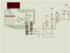
i need somebody help me checking the circuit diagram in the attachment.
The signal is 0.024V into ad620 (Actually this is load cell output signal), ad706 played the role of a voltage follower, The amplified signal from ad620 directly into mcu ATmega16L, then dispaly on the LED.
I don't know this circuit is properly connected or not. i am a new people in this area, really want get your help, thank you very much!
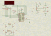
 D4
D4