Gopal Adhikari
New Member
Dear all,
I am trying to design a two stage opamp. I have gone through texts to equip with basic ideas to design a opamp. The problem is dont know how to choose the ICMR Values and the values of Vth1max, Vth1 min, Vth3max. The Design Procedure i used is as follows.
(μnCox≈246.74 and μpcox≈92.75 * I have calculated using the model file please suggest if I am correct)
Specifications
Gain>=60dB
Power Supply : ±1.8V
GBW=5MHZ
PM>=60°
SR>=10V/μs
CLoad=10Pf
ICMR= ± 1.6V
________________________________________________________________
| at Vin = - 1.6 , Vth1min = 0.31 Vth3min = 0.432 |
| at Vin = + 1.6 , Vth1max = 0.622 Vth3max = 0.433 |
| These values are found using the simulation of the |
| diff amp in the Circuit shown in the opamp.asy file |
| I hope the values are correct. |
|_______________________________________________________________|
Design
1. Cc=0.22*CLoad=2.2pF ≈3pf(adjusted)
2. I5=SR*Cc= 10*3= 30μ
3. gm1=GBW*Cc*2π=94.24μ
4. (W/L)3 = I5/(μpCox[VDD-ICMRmax-Vth3max+Vt1min]^2)
5. VDSSAT5 = ICMRmin-VSS-√(I5/β1)-Vth1max
6. gm6 = 10*gm1 =942.4μ
7. I6 = ((W/L)6*I4)/(W/L)4 = 36.38 ≈36
Using These Values I have simulated the circuit. With these values I assume that the Gain should be >60dB. but I am getting just above -10dB. What am I Doing Wrong. I am stuck, Please suggest me what should I do? I also need to simulate the settling time, psrr, open loop gain and closed loop gain and other parameters of opamp using LTSPICE. please suggest how can I do that too.
Also, When I simulate using ground instead of VSS, I get gain >60dB. ??
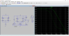
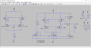
I am sorry , the mosfets are named badly in the picture but in the schematics file, its named correctly.
Hope I will be helped
I am trying to design a two stage opamp. I have gone through texts to equip with basic ideas to design a opamp. The problem is dont know how to choose the ICMR Values and the values of Vth1max, Vth1 min, Vth3max. The Design Procedure i used is as follows.
(μnCox≈246.74 and μpcox≈92.75 * I have calculated using the model file please suggest if I am correct)
Specifications
Gain>=60dB
Power Supply : ±1.8V
GBW=5MHZ
PM>=60°
SR>=10V/μs
CLoad=10Pf
ICMR= ± 1.6V
________________________________________________________________
| at Vin = - 1.6 , Vth1min = 0.31 Vth3min = 0.432 |
| at Vin = + 1.6 , Vth1max = 0.622 Vth3max = 0.433 |
| These values are found using the simulation of the |
| diff amp in the Circuit shown in the opamp.asy file |
| I hope the values are correct. |
|_______________________________________________________________|
Design
1. Cc=0.22*CLoad=2.2pF ≈3pf(adjusted)
2. I5=SR*Cc= 10*3= 30μ
3. gm1=GBW*Cc*2π=94.24μ
(W/L)1= gm1^2/(μnCox*I5)= 94.25^2/(246.79*30)=1.2
=30/(92.75[1.8-1.6-0.433+0.31]^2) =54.55 ≈ 54
= -1.6+1.8-0.3182-0.622 = -0.103722 * I am confused about this value as VDSsat5 should be above 100mV
(W/L)5 = (2*I5/(μnCox*VDSsat5^2)) = 22.91 ≈ 23
(W/L)5 = (2*I5/(μnCox*VDSsat5^2)) = 22.91 ≈ 23
gm4 = √(2*I4*μpCox*(W/L)4) = 387.62μ
(W/L)6 = (gm6*(W/L)4)/gm4 = 131.28 ≈131
(W/L)6 = (gm6*(W/L)4)/gm4 = 131.28 ≈131
(W/L)7 = (I7*(W/L)5)/ I5 = 27.89 ≈ 28
Using These Values I have simulated the circuit. With these values I assume that the Gain should be >60dB. but I am getting just above -10dB. What am I Doing Wrong. I am stuck, Please suggest me what should I do? I also need to simulate the settling time, psrr, open loop gain and closed loop gain and other parameters of opamp using LTSPICE. please suggest how can I do that too.
Also, When I simulate using ground instead of VSS, I get gain >60dB. ??
I am sorry , the mosfets are named badly in the picture but in the schematics file, its named correctly.
Hope I will be helped
Attachments
Last edited:
")