Electro Tech is an online community (with over 170,000 members) who enjoy talking about and building electronic circuits, projects and gadgets. To participate you need to register. Registration is free. Click here to register now.
Welcome to our site! Electro Tech is an online community (with over 170,000 members) who enjoy talking about and building electronic circuits, projects and gadgets. To participate you need to register. Registration is free. Click here to register now.
Found some interesting reading about band pass filter design.
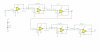
Using FILTERPRO I cascaded a low pass (300hz - 1500hz) with a high pass (1200 - 7k) thus ending up with a 300hz to 7khz filter.
THEN got to thinking, why use two separate filters?
Just one filter w/ an audio limiter section and add two output amps (left ear/right ear.)
the ideal design would be two individual filter sections but ?
Need to look at cost etc.
need to add the audio limiter and amp then simulate
Found some interesting reading about band pass filter design.
Using FILTERPRO I cascaded a low pass (300hz - 1500hz) with a high pass (1200 - 7k) thus ending up with a 300hz to 7khz filter.
THEN got to thinking, why use two separate filters?
Just one filter w/ an audio limiter section and add two output amps (left ear/right ear.)
the ideal design would be two individual filter sections but ?
Need to look at cost etc.
need to add the audio limiter and amp then simulate
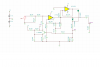
It is a first order lowpass then a second order lowpass (why not use a third order lowpass instead that uses only one opamp?) then another second order lowpass.
Then it has a first order highpass then a second order highpass (why not use a third order lowpass instead that uses only one opamp?) then another second order highpass.
It is almost the same as you had before except its fifth order filters have steeper slopes than your second order filters before.
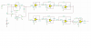
Sorry, but I guess you don't understand how transistors work.
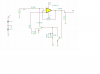
You have the PNP transistor in the limiter connected completely ass-backwards. Its collector is supposed to pull the gate of the Jfet to 0V for the Jfet to turn on and attenuate an input signal that is too high.
I don't know the impedance of your earphones and I don't know how much sound level boost at what frequencies your deafness needs. Then I don't know if an opamp can provide enough power.
On the forums, two other guys are making hearing aids. They are using a three-band tone controls circuit as an equalizer because most people who were deafened by guns or acid rock music have a loss of high frequency sensitivity. I told them to see an ear doctor to find out if boosting the levels with a DIY hearing aid might destroy their remaining hearing.
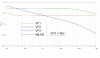
I can't get 0V on the VF1 output.
The orginal design showed a 20mv-20v input = 25mv output
Tried swapping op amp inputs etc. Still can't get output to 0v to turn on the PNP transistor.
I shorted across (grounded the jfet base) just to verify if the circuit actually works.
un shorted -215db
shorted -15db
must work but going to try the lm741 op amp in orginal circuit but it shouldn't make any difference?
Without a signal, R1 causes the base of the PNP transistor to be 0V so it is turned off.
When the peak of the output signal reaches about -0.6V then the PNP transistor will begin to turn on and will cause the Jfet to begin turning on to prevent the signal from being at a higher level.
Still can't get output to 0v to turn on the PNP transistor.
0V on its base completely turns it OFF, not on. It turns on when its base is -0.6V to -0.8V.
I shorted across (grounded the jfet base) just to verify if the circuit actually works.
I shorted across (grounded the jfet base) just to verify if the circuit actually works.
un shorted -215db
shorted -15db
That is backwards. When the gate of the N-channel Jfet is grounded then it would have turned on and attenuated the signal.
But your Jfet has no part number so the simulation program doesn't know what is going on.
must work but going to try the lm741 op amp in orginal circuit but it shouldn't make any difference?
An LM741 is a 43 years old piece of garbage. It is noisy (hiss) and has a poor high frequency response (only 9kHz at full output).
It was designed to use ONLY a 30V supply so many do not work when the supply is only 10V and your supply is much less.
The jfet might be the wrong type. Its a 2n5459--need to check.
I realize that when the op amp output drops below .6 or so the PNP turns on thus grounding the Jfet base
If the Jfet is wrong type then the Jfet won't wrok right.
Will check schematic over and recheck voltages.
I think you hit the nail on the head about the jeft might be the wrong type.
A 2N5459 Jfet is an N-channel. It is cutoff (turned off) when its gate voltage is from -2.0V to -8.0V so most will not be cutoff since your negative supply is only -4.15V.
A 2N5457 Jfet is cutoff when its gate voltage is "only" from -0.5V to -6.0V.
tried several things but can't get the PNP to ground the Jfet base.
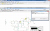
Going to try this circuit again but now I keep getting an error
Its one thing after another.
Needed a return to ground
Back to using this circuit but thinking I am missing something. When I view the signal analysis exactly what am I looking for to determine if the circuit is working properly?
I get the impression that the wave form should be lower or at zero when it lowers the signal level (volume)
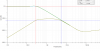
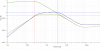
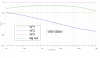
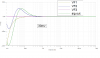
Trying to include a varying sine wave voltage from 20mv to 30v in 5 steps but not sure I got it right, so I view wave w/ 3v then with 30 volts. Both look the same?
My biggest problem is what to lok for?
here are the two different wave forms, one using 30mv signal and one using 30v signal(VG1)
Looking at these two different pictures I THINK I see where the output drops off?
Here is the project for the Fast Peak Limiter circuit: **broken link removed**
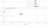
Its specs say that it limits the output level from rising above 1.65V RMS, has a max attenuation of 40dB (100 times) for extremely high level inputs and has maximum gain of only 6.8 for low level inputs.
Since it has a gain of only 6.8 then a signal at the input of more than 243mV RMS or 343mV peak will cause the output not to exceed 1.65V RMS or 2.33V peak.
Yes, a 3V and a 30V input will produce the same output 1.65V level.
Whats the story on the control voltage?
I thought about applying say 2v to this but?
I can change the sine wave amplitude but would this indicate a drop in the output sig out?
OR just leave well enough alone? (I was thinking of using ONE FAST AUDIO PEAK LIMITER, ONE set of BP filters and two amp outputs? but perhaps two separate bP filters (one for each ear that I can tune?
The rectifiers make the control voltage for the fast audio Peak Limiter. They charge the filter capacitor quickly for a fast attack at limiting the level and have a high value resistor to discharge the capacitor slowly for the limiting to be reduced or eliminated for low level sounds.
A loud sound causes the output of the limiter circuit not to exceed 1.65V RMS. The output is not reduced, it is limited.
Instead of bandpass filters I think you need at least 3-band tone controls. You can boost a band or two where your hearing needs it (probably high frequencies) and cut the 3rd band if you need it.
Instead of a Peak Limiter I think you need an automatic volume control circuit that amplifies low levels and limits high levels with a fast change between them.
This site uses cookies to help personalise content, tailor your experience and to keep you logged in if you register.
By continuing to use this site, you are consenting to our use of cookies.