Continue to Site

Welcome to our site!

Electro Tech is an online community (with over 170,000 members) who enjoy talking about and building electronic circuits, projects and gadgets. To participate you need to register. Registration is free. Click here to register now.

  • Welcome to our site! Electro Tech is an online community (with over 170,000 members) who enjoy talking about and building electronic circuits, projects and gadgets. To participate you need to register. Registration is free. Click here to register now.

Generating uni-polar PWM signal using IR2113

Status
Not open for further replies.
All modern pure sinewave inverters use a micro-controller to make the PWM and make some dead time.
Since you are making an old fashioned inverter then maybe dead time does not matter.

Without deadtime the output transistors both turn on for a moment as they switch states which increases the battery current and heats the output transistors. It is most noticeable when the inverter is idling with no load.
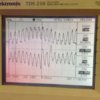
 
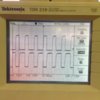
So I connect the Hin(A) into both HIN and LIN of IR2113 and this is the waveform that I got. But still, it's not working.
 

Attachments

  • TP(IGBT1HIGH),TP(IGBT2LOW)-(1).jpg
    TP(IGBT1HIGH),TP(IGBT2LOW)-(1).jpg
    1 MB · Views: 897
Your new waveforms are not rectangular PWM, instead they are an odd-looking high frequency mixed with a low frequency. Also they do not swing from 0VDC to +12VDC.
A good thing is that the timing shows that both IGBT's are not turned on at the same time anymore.
 
Your new waveforms are not rectangular PWM, instead they are an odd-looking high frequency mixed with a low frequency. Also they do not swing from 0VDC to +12VDC.
A good thing is that the timing shows that both IGBT's are not turned on at the same time anymore.
However, this is the signal that I am inserting to the gate driver. Could it be somewhere went wrong?
 

Attachments

  • TP(HINA),TP(LINA).jpg
    TP(HINA),TP(LINA).jpg
    1 MB · Views: 1,028
In post #122 you used the same signal for Hin and Lin and the IGBT's correctly both did not turn on at the same time.
But in post #124 the signals look pretty good but one of the signals is inverted. Why?
 
NONE of the circuits in Google use a negative supply for the LOW output transistor but you do. They all connect the source or emitter pin to the COM and VSS pins of the IR2113. Try it.
 
As you know, the DC power supply has a red and black node.For the first DC power supply, it is powering up my IC chips in the circuit. Therefore, the red node is a +12V and the black node is 'GND'
For the second DC supply, it is connected to the IGBT with the red node as +12V and black node as 'GND2'. When I connect both the GND and GND2 together, the DC power supply goes haywire. 'The voltage reading of the first DC power supply keep rising till very high"

Sorry that I am not that good in this area..
 
Perhaps one of those power supplies should be connected such that red=GND, black=-12V ?
 
Look at the many sinewave inverters using the IR2113 driver IC in Google. NONE of them use a positive and negative supply for the output devices, the LOW device is connected to COM and VSS which are the circuit's ground. But the inverter circuit in this thread has the LOW device connected to -12V and the power supply voltages have almost the same signal on them as the output.

I suggested to GET RID of the -12V supply but maybe he simply shorted its output.

Why are there TWO 12V power supplies anyway? Why are there TWO grounds in the circuit, GND and GND2?

Post #87 and post #94 have the latest schematic. They do not have two grounds. Also, they have the LOW devices connected to -12V which is wrong.
 
Why are there TWO 12V power supplies anyway?
Why indeed? The thread title refers to uni-polar PWM.
 
Also there are no steering diodes in the circuit. The examples given in the book "Power Electronics" by N. Mohan, show that there are four steering diodes and that The high side of 'A' is on at the same time as the low side of'B'. And viceversa for the high of' 'B' and low of 'A'.

And that only the low side switches are PWMed.
 
Also there are no steering diodes in the circuit. The examples given in the book "Power Electronics" by N. Mohan, show that there are four steering diodes and that The high side of 'A' is on at the same time as the low side of'B'. And viceversa for the high of' 'B' and low of 'A'.
"Steering diodes" are not used in an IR2113 circuit. It has "boostrap diodes" to boost the drive voltage to the upper followers.

only the low side switches are PWMed.
That does not make sense. If the high pulse is narrow then the low pulse should be wide. If the high pulse is wide then the low pulse should be narrow.
 
The steering diodes are missing in the output section of the circuit.

Are you saying that PWM should be used on both high and low side?

I'll scan and post the circuit in the book.
 
PWM is a rectangular waveform that goes up and goes down. Its output goes up when the upper device has a positive input because it is a follower that does not invert.
Its output goes down when the lower device has a positive input because it inverts.
PWM is the ENTIRE waveform, not just the top part so of course PWM is also on the low side but it is the opposite of the width at the high side.
 
Here is a copy from the book. The text under it says bipolar because that's the next circuit they talk about, but the illustration is for a unipolar.
 

Attachments

  • inverter038.jpg
    inverter038.jpg
    525.3 KB · Views: 874
The text from your book is too small and too fuzzy to read. The waveforms look like ordinary PWM and it is made with a low frequency sinewave and a high frequency triangle wave both feeding a comparator just like in this thread. The output devices are a bridge to effectively double the voltage swing.

The top of the PWM gets wider while the bottom gets narrower then when the top gets narrower the bottom gets wider like I said.
 
Look at the many sinewave inverters using the IR2113 driver IC in Google. NONE of them use a positive and negative supply for the output devices, the LOW device is connected to COM and VSS which are the circuit's ground. But the inverter circuit in this thread has the LOW device connected to -12V and the power supply voltages have almost the same signal on them as the output.

I suggested to GET RID of the -12V supply but maybe he simply shorted its output.

Why are there TWO 12V power supplies anyway? Why are there TWO grounds in the circuit, GND and GND2?

Post #87 and post #94 have the latest schematic. They do not have two grounds. Also, they have the LOW devices connected to -12V which is wrong.

Sorry for the confusion.
For the DC supply for the IGBT, it is operating from a different power supply. [+VDC, GND]
To power up all my IC chips, it is currently using a DC-DC converter. [+12V and GND]
In conclusion, there is 2 supply sources. One is to power up the IC chips only. While the other one is powering up the IGBT for the switching.

However, I cannot connect both of these 2 ground together. Once I connect it, my power supply for IGBT goes haywire. I edited my schematic as the TP(HINA)&TP(LINB) complimentary with each other and TP(HINB) and TP(LINA) are complimentary as well.

For my schematic, IGBT1HIGH will be switching with IGBT4LOW while IGBT3HIGH is switching with IGBT2LOW.
I had also changed the value of the gate resistors as well as the bootstrapping capacitor according to the values I calculated.

As the IGBT i am using is TO-220FP, GF10NC60HD. Could it be that the IGBT is not compatible.
 

Attachments

  • SPWM(VCC&GND).pdf
    54 KB · Views: 818
However, I cannot connect both of these 2 ground together. Once I connect it, my power supply for IGBT goes haywire.
I think you need to check the specs/datasheets for the two supplies and find out why that happens. Why can't you power the IC chips from the same supply as the IBGTs (via a voltage regulator if necessary to get a lower voltage)?
 
You have one IR2113 driving the upper IGBT of one output and the other IR2113 driving the lower IGBT of this output which is VERY unusual. It will work exactly the same as before (wrongly) but it is very confusing to look at. You want each output to drive push-pull and look like it.

I think you do not understand what a bridge output does and how it works. It is supposed to DOUBLE the voltage swing because when one output goes up then the other output goes down. Then the comparator for the IR2113 for one one output must have the low frequency sinewave inverted.

I corrected your schematic and I am just guessing that it will work properly:
 

Attachments

  • sinewave inverter guess 1.png
    sinewave inverter guess 1.png
    69 KB · Views: 5,387
Status
Not open for further replies.

Latest threads

Back
Top