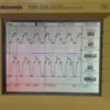
I think you are WRONG.But only the Lin should be PWMed. If there is no constant DC on the Hin, there is no voltage to control the bootstrap part of the circuit.
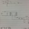
The high-side IGBT must be driven so that its source charges the capacitor to a voltage ABOVE the supply voltage so that the gate voltage pulse is about 10V higher than the source voltage.
It is a charge-pump.
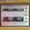
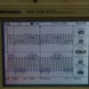
The power supply is a mess and I don't know why it is not fixed or replaced.
I have a suspicion that the L-in must not be inverted because when it goes high you want the low-side IGBT to turn on and pull the output down.