Electro Tech is an online community (with over 170,000 members) who enjoy talking about and building electronic circuits, projects and gadgets. To participate you need to register. Registration is free. Click here to register now.
Welcome to our site! Electro Tech is an online community (with over 170,000 members) who enjoy talking about and building electronic circuits, projects and gadgets. To participate you need to register. Registration is free. Click here to register now.
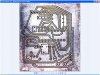
Here my first try at it I think it came out very well all but the bottom ground. **broken link removed**
And with all the parts on the front side. I don't think it to bad for reusing some old copper. **broken link removed**
That looks like a highly classified Thing - A - Ma Jig for controlling a What ya ma call it with a hoo dickiy
LOL
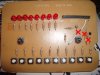
no really I think its an ADC / PIC test board.All them pots gave it away.
looks like your using the yellow colored solder flux??
hope you covered the traces w/ clear coating of laquer or ??
I am planning on building a test board myself.
I assume the header plugs into the 8 pos socket on a Junebug??(the clone you built)
what I want to find is some pre assembled ribbon cables 8 cond and 5 cond.
you have a schematic I could use for suggestions?? on building a test board.
presently I have an 18 pin socket with 4 LEDS, 4 resistors for the leds , a diode and resistor for the PIC and a 5 pos header.
I like to place a sacrificial wide line around the entire design. Many times the line will fail to transfer/etch but the rest of the design will be perfect.
I like to place a sacrificial wide line around the entire design. Many times the line will fail to transfer/etch but the rest of the design will be perfect.
Or take a fat sharpie around the outside edges of the board. I used to do that to stretch the ferric chloride life (I would color in any large areas as well or polygon them in Eagle) and it speeds thing up a little.
Heat all over is key for sure.
I need to get one of those cool made in China stamps though.
The CNC I use for drilling requires room on the bare PCB for clamping. The extra board makes the PCBs a bit easier to handle/process. I use cheap box tape to mask over the unused area to save on etchant.
I also use it to mask the other side when I etch one side at a time.
I increase the distance from traces to ground planes.
then only the space between the trace and plane are etched.
also found using a thin board so that light can be seen in the etched areas so any shorts or trace breaks can be seen very clearly when held up to a light.
the board pictured has liquid tin applied.
It seemed to make soldering easier.
Well how about an educated guess... Everything about ultrasonic cleaners is optimised to focus all the power on removing stuff from surfaces... It may not be the best agitator for an etchant tank.
Believe me I don't even like educated guesses.
This will be tried shortly and that is not a guess, educated or other vise.
Ultrasonic cleaners are all about getting the transducers energy transfered into the liquid, it does not focus ALL the power to stuff on the surface.
That's right, a small percentage is lost as heat in the liquid. But they are pretty efficient at transferring the power to the surfaces being cleaned.
Hey I didnt say it wouldn't work... Just that it might not be the best agitator.
The commercial systems (like in the PCB house) stand the board vertically and pump hot etchant to the top of the PCB to drench it in a constant flow. Thats gonna remove the copper, bubbles, and fouled etchant very well WITHOUT stressing the mask too much.
The way i etch PCBs is to put the board in an approx 10x3inch icecream box(plastic) about 3 inces thick.Pour hot(electric kettle for best result) water on it, some chunks of FeCl(even this is hard to get where i live).Close the lid and move the box like a see saw so as to make the etchent flow on the surface to and frow. Gives a PCB with in 2 to 3 minutes. Cheap and easy.
The way i etch PCBs is to put the board in an approx 10x3inch icecream box(plastic) about 3 inces thick.Pour hot(electric kettle for best result) water on it, some chunks of FeCl(even this is hard to get where i live).Close the lid and move the box like a see saw so as to make the etchent flow on the surface to and frow. Gives a PCB with in 2 to 3 minutes. Cheap and easy.
I use Muriatic Acid / Hydrogen Peroxide and have always been afraid or heating it because of the corrosive fumes. Had a friend once that ruined a shop full of tools, don't know what he used for enchant.
That is impressive etching times, thanks for posting. Now we know what we have to strive for.
P.S. About toner transfer DIY paper, I am going to test the heavy duty wax paper used by butchers; have not got any yet. I am also going to test the bag that some breakfast serials comes in.
P.S. About toner transfer DIY paper, I am going to test the heavy duty wax paper used by butchers; have not got any yet. I am also going to test the bag that some breakfast serials comes in.
You are a man on a mission . I would tell you not to bother because all these things have been tried, but the the composition of the coatings may have changed since anyone gave them a shot.
You are a man on a mission . I would tell you not to bother because all these things have been tried, but the the composition of the coatings may have changed since anyone gave them a shot.
Please don't be offended and take this as constructive criticism.
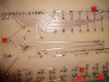
I know this is your first attempt, good it works but next time I'd advise neatening it up a lot, it's far too sloppy. If I designed a PCB like that at work they would tell me to do it again; it wouldn't even be allowed to be manufactured, it would have been rejected at the design phase.
The resistors should all be mounted straight (preferably at right angles) with the leads perfectly straight and no wiggly bits.
What's with the copper wire?
Did you forget to put the traces on? Fair enough these sorts of modifications might be necessary at prototyping phase but it certainly shouldn't be part of the design.
Those holes are far too near the pads, traces and components. You should allow enough room for error when drilling and for any fixings you plan to use: nuts, washers, screws etc.
Also try to make the tracks at 90° or 45° angles and avoid tight corners which tend to etch poorly.
I've put crosses through all the really bad parts. To be honest the rest isn't much better but most could be fixed by forming the component leads correctly and better soldering technique. You've probably got many poor solder joints whcih can't be seen on the photo.
Unfortunately I couldn't find any tutorials that go into lead forming as much as I'd like.
I tend to make the ¼W resistor leads 0.4" (about 10mm) pitch so I can use veroboard as a forming jig.
You might think I'm being picky but it's important to do a reasonably neat job otherwise fault finding can be very difficult: bad joints can be open circuit and crooked connections can easily short circuit. You want to minimise that risk of errors not maximise it.
reusing a old used board IMHO it looks pretty good.
not as good as if the board was from scratch.
I myself plan on building a test board from scratch.
just need a schematic of something that already works.
why reinvent the wheel??
My second etch with the Muriatic Acid/Peroxide didn't go so well. It seems to have lost all it's etching ability. I ended up adding more peroxide after 15 minutes and heating it up a bit. I've got the tank left open right now to evaporate it off some and concentrate it a bit.
It worked, but it ate under the etch resist on my poor board, so it looks like it has a rash.
Seriously, have you been drinking colloidal silver?
Even if I overlook that, it's still a pretty shoddy job. What's going on with the resistor with the long scruffy leads stretching from one side of the PCB to the other?
It's a obviously a PCB design fault; that can be fixed but it won't be pretty.
If I did not have the option of making a new PCB (which I would do if possible) I would have drilled another hole, mounted the resistor straight and tacked some insulated hook-up wire to make the connection on the other side. If I wasn't allowed to drill a new hole, I would have covered the resistor with clear heatshrink to stop it from shorting.
Using an old board is no excuse for such poor workmanship.
If the board is old then it doesn't appear to have been properly cleaned before reusing it. As much of the excess solder as possible should have been removed (using a solder sucker and desolder braid) and the whole thing should have been washed in alcohol to get rid of the remaining flux.
Again, as I said before, some of the solder joints appear to be poor but it's not that clear looking at the tiny picture.
BE did say it was his first try. It may not be great looking but you need to give him credit for getting it done. More then a few people never get this far.
If people get too much crap about their efforts they will not post them.
^ I tried out your Pulsar paper. I'll have a review later. Unfortunately the final board is a little rough looking due to the problem with the etchant.
hero999 you anit hurt my feeling the board had the holes in it when I found it.
It came off a motor controller and i sanded off where four wires was solder to it and reused it just to try it out never did it before the one hole on the right hit where two
resistors went and the jumper I forgot to run the ground to the header I like junk have a basement full of it. and plan to use it some where. LOL
This site uses cookies to help personalise content, tailor your experience and to keep you logged in if you register.
By continuing to use this site, you are consenting to our use of cookies.