Space Varmint
New Member
RadioRon & I were discussing digital frequencies control solutions in another thread about radio transmission & reception and kind of decided that the topic deserved it's own category. So I figured I would start here and post an old single loop PLL circuit. In here we hope to get input from anyone who has a good suggestions or just some research you have come across. Anything about digital frequency controls. Pros & cons of various techniques. Recent breakthroughs. Even old theory and descriptions for the newbies.
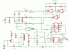
The circuit below though it is a working PLL (Phase Lock Loop) digital frequency synthesizer, it is being used to describe the basic components of PLL. Q1 is configured into a Hartley oscillator. This is where the output from the frequency synthesizer is produced and fed to the radio circuits as the oscillator. In this circuit the oscillator is running at 400 MHz. Because the oscillator is running at such a high frequency, it is necessary to divide the frequency down to something that is workable for the TTL to used later. This is the job of U2 which is a prescaler. A prescaler is nothing more then a counter being used as a frequency divider except for one thing. It is composed of ECL (Emitter Coupled Logic) which is transistors configured in common-collector or emitter-follower arrangement. The reason for this is, transistors switch much faster in this type of arrangement. Overall it it just a divide by 10 counter.
So now the output of the prescaler is 40 MHz is being fed to a much cheaper TTL counter which is being used as a divide by 16 divider. This leaves us with an output of 2.5 MHz. This is fed to the comparator. This is a rather old type of frequency comparator. Now days IC's are available that use a combination of XOR gates and flip-flops that can do more than just detect phase shifts but also can detect frequency to the point that a PLL can lock up on a harmonic frequency of say, times 2 but the steering logic in more modern phase detectors/comparators will prevent this phenomena.
Now we need a stable reference frequency and as we all know a crystal can be quite stable, so we build a crystal oscillator. IC1a & IC1b make a good cheap & dirty square-wave oscillator and we can use gate IC1c as a 180 degrees phase shift for the comparator. You may use a sign-wave oscillator as well here.
So we feed the divided down oscillator signal and the reference oscillator signal to the comparator or phase detector and both are at the same frequency only one of the signals is crystal locked. In most of your phase detectors you usually only need these two signals, but this type here requires a 180 degrees phase shifted signal as well. It is an old comparator circuit and is a rare bird these days. Often times you can use just these two signals going to an XOR gate and will work the same.
The output of the phase detector will be a chopped up AC signal of the two original signals (divided down oscillator/VCO & reference osc). The average voltage of the AC signal will shift up and down very quickly as the VCO (oscillator) frequency drifts higher or lower then the reference frequency times the division factor. Visualize them running at same frequency for all practical purposes. This being the primary voltage of interest, also known as "error DC", we can amplify this signal with a DC amplifier. A DC amplifier is an amplifier with no coupling or bypass capacitors. We do not want to block the DC.
Being that this is still an AC signal, we do not want to apply it to the VCO yet or it will cause the VCO to jump all over the place. We are only interested in the overall average voltage of "error DC". R7 & C8 compose a simple "loop fiter" to smooth out the AC and create an average DC.
No we see that the output of the loop filter is applied to the varactor diode of the main oscillator. The varactor being in the tank circuit of the oscillator makes it a VCO (Voltage Controlled Oscillator) since the varactor will change it's spacing across the juction of the diode, effectively changing it's capacitance. Now we have a way for the feedback loop to self adjust any drift that may occur by comparing to the locked signal from the crystal reference frequency.
This is a description of the basic lock loop. The frequency can be changed in a number of ways. In the case of this circuit, one method might be to jam load the counter U1 with a divide by 15 count instead of divide by 16. This will cause the frequency to jump down 2.5 MHz. The step rate is determined by the reference frequency where it is applied to the phase detector. Had we divided both signals down by an additional divide by 10 and then apply the signals to the phase detector, the step rate would be 250 KHz.
So these are the basic building blocks of a PLL digital frequency synthesizer. Then there is another commonly use technique referred to as DDS (Direct Digital Synthesis) where the actual oscillator frequency is built by digital D to A converters.
Any input is welcome. The object will be some of the most efficient superior techniques known today but we do not want to leave out any of the history of signal processing.
Attachments
Last edited:
")
