Electro Tech is an online community (with over 170,000 members) who enjoy talking about and building electronic circuits, projects and gadgets. To participate you need to register. Registration is free. Click here to register now.
Welcome to our site! Electro Tech is an online community (with over 170,000 members) who enjoy talking about and building electronic circuits, projects and gadgets. To participate you need to register. Registration is free. Click here to register now.
Please do not save or post anything electronic as a Jpeg or JPG file type because it has high compression that messes up straight lines and makes a fuzzy mess around things. Use a PNG file type instead so it will be very clear.
You have somethings duplicated and a voltage statement that should not be on your simulation:
Not sure how your capturing you screen shots, but they are too difficult to read. Windows comes with a nice screen capture tool, and you can just snip the areas of interest thus reducing screen size.
I am hesitant to make any recommendations to you for board fab houses. You tend to blame others for your errors - I don't want to bare any responsibility for failure of a poorly designed board, nor do I want my vendors bad-mouthed for providing exactly what you ordered.
That being said, the vendors I currently use are Smart Prototyping and Elecrow Electronics. I have used both these services extensively with excellent results. Depending on exactly what you want, you may be able to find slightly cheaper prices elsewhere, but these two vendors are a proven reliable source.
have never bad mouthed a vendor.
blame others??
thanks for the vendors. I was maybe going w/ PCBWAY but going to try out smart prototyping. Hopefully shipping is reasonable.
Mr Deb there is cheaper places you can use like dirty PCB, but first lets get the design done before we worry about boards. You dont order furniture to fill a house before you have brought one do you?
yes but we are going to play nicely, so Mr Deb can do his drawings and 'designs' then we will do it properly, get it working and ......................walk away unscathed....
Anyway too early to tell much yet we are only on page 5, another 40 or so to go yet before we get started designing. Dont worry Jonsea it will be ok , I have a reason to have a go at doing this, I will plonk my drawings and code here and if Mr Deb wants to experiment with it after that I dont mind, but once I get it working I wont be able to alter much as I dont have time.
As for cap touch switches I am figuring 3 and they can operate a menu system, so up and down menu and select. I *might* add a cap slider, I have dev boards for 8051 and gecko 32 chips and cap touch but havnt messed with pic cap touch yet. Shouldnt be too bad and if it is then menu system and momentary switches. Filter for leds etc he can add on later if he likes, I dont need that but the general design should be the same. Also need to keep the board a reasonable size, I am making mine but if he is buying some in then better keep it small or the cost gets silly for wasted space
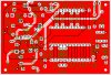
NO WORRY guys, the board I posted was not the final design. I added a bottom ground plain, wider clearances and mounting holes.
As I mentioned the design I found needs to ferment before finalizing.. As for the traces, .008 for most of them. Power traces are wider.
Just because the software lets you use 8 mil track widths doesn't mean it's a good idea. 8 mil is pushing the limits of what a cheap fab house can do. If you're laying out a high density surface mount board, you may need to use 8 mil traces, but unless you absolutely need such thin traces for clearance, it's prudent to use larger trace widths.
Your board is not that dense. There's plenty of room for 16 mil or larger traces, and for power and ground, I'd suggest even larger.
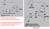
This chart is Elecrow's PCB specifications. It shows that they can make boards with 6 mil trace & space.
However, they recommend greater than 8 mil trace and space. Neglecting all considerations other than what will fit on the board, 16 mil or even wider traces will not be a problem to fit.
I would suggest making your power and ground traces bigger... nevermind, I already have on 3 occasions.
Your 555 chip would work better with a Vcc connection and the floating island of a ground plane (well, almost an island with a single 12 mil connection) would be much improved if some things were moved slightly.
I won't comment farther than that, since laying out a board before the circuit is finalized is... [redacted]
One problem I have is keeping enough clearance around mounting holes. I've solved that problem by creating a part in Eagle showing the size of a 4-40 nut (which is close to the size of a 3mm nut) with the area needed for a nut driver around it. Ideally, you want to keep component mounting holes out of the entire area to ensure you have enough room to screw a nut down. Ideally, I try to keep traces out of the nut area and the tool area too if possible, since the only insulation between the nut and any traces is just the soldermask. A rough face on the nut and you could have traces shorted to the mounting hardware and each other.
Jonsea your ground trace goes off the board!! how is the fab house sposed to do that? . And hate to burst any bubbles but I am making my board by laser printer so the traces will be the smallest i can do without hair tearing, so around 12 mil min for smallest.
I might use a marker pen by hand now I have seen how effective jonsea's method is lol
This site uses cookies to help personalise content, tailor your experience and to keep you logged in if you register.
By continuing to use this site, you are consenting to our use of cookies.