Electro Tech is an online community (with over 170,000 members) who enjoy talking about and building electronic circuits, projects and gadgets. To participate you need to register. Registration is free. Click here to register now.
Welcome to our site! Electro Tech is an online community (with over 170,000 members) who enjoy talking about and building electronic circuits, projects and gadgets. To participate you need to register. Registration is free. Click here to register now.
hi Can,
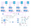
Its advisable that on the CMOS IC inputs that have switches you have a pull up resistor.
For example the Up/Dn,, connect the CMOS input to +5V via a 10k resistor,, when the switch is Open the Up/Dn line is High and when the switch is Closed the Up/Dn line is 0V.
You do not need a change over toggle switch.
OK.?
EDIT:
Look at this edited image, note the two 10K's also the Load pins are at 0v.
You also need another 10K on the Left side pair of counters on the clock
No problem, not spam, just lots of iterations to try and get it right.
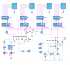
Your latest version looks much better, it is possible to see what is going on in the circuit at a quick glance.
Keep up the good work, you are getting there.
hi again,
Remove the diode on pin 3 of the 555, there are other areas which could be improved.
Sorry about the piece meal posting, but it takes some time to look thru your diagram.
E
Thanks guys for all the help
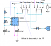
The diode on the output pin of the 555 timer needs to be there else when preseting the time for the both players (both players) it won't work..
The software I am using also has a simulation mode where you can test out the circuit
Also, would I need to put any capacitor randomly in the circuit to smooth it out, if so where and why (I don't really get why you need then in the circuit so it would be fantastic to know). Thanks guys
Oh and your question... 'what is the switch for?' When pressed there are two possible modes... First mode is driven by the 555 timer with pulses of about 1 second apart then the second mode is when you want to select a preset for the chess timer.
This is how you would do that..
-Once the chess timer has power no inputs or anything will be possible until the 'Input Allower' button is pressed. Once that is done you can press the 'pulse' button which sends one pulse to one of the timers (Depending what side the 'Swap Player' switch is switched and if the 'Start Timer/Select Time' switch is on the Select time mode (side)...
After you have slected the time for both timers then you can proceed to press the 'Start Timer/Select Time' which will change the outputs of the display drivers to be run with the 555 timer..
Also, would I need to put any capacitor randomly in the circuit to smooth it out, if so where and why (I don't really get why you need then in the circuit so it would be fantastic to know).
That actually depends. If IC require low voltage ripple to work properly, it is advisable to place it between VCC and VSS (closest to these IC pins). If not, I would not bother with adding more complexity. Required with sensitive ICs as MCU, memory chips, etc.
As well, anti-bouncing circuit is perhaps necessary around certain critical buttons.
Hi, i'm gaving a few more issues. This incudes;
When the Pulse button is spammed (to count down or up on one of displays (depending what why the Down/up switch is pressed) it randomly resets everything... I have noticed If I send a pulse within a pulse it does this, how can this be fixed?
On more question, I have install some Nor gates connected to the 4511 IC so when the 1 st and 3rd 7 segment displays a zero which will concenquelly switch on the LED at the top (Depending which side is zero)... The led is only getting 3.6mA and 1.6V, is that sufficent?
Thanks for any advice
Can your simulation software apply unique designators to the parts in your schematic? There are a few comments that I would like to make but it is difficult to do so without being able to call out an individual part.
But one comments about somethings that might simulate OK, but may not work properly in hardware is:
Floating inputs. (neither high nor low) Particularly when you use diodes and switches in your logic path. For example, two of the CD4510 clock inputs that are feed from a switch and a diode. The counter connected to the open pole of the switch will always be floating. The counter connected to the closed side of the switch will be floating when the state on the other side of the two diodes feeding that net is LOW (the diodes are not froward biased and are therefore open connections). If your circuit is simulating OK, then the software is set to treat a floating node is a logic LOW. In real hardware you need to ensure that a floating input is in a KNOWN default state. Use a resistor on each of these two inputs to ensure the state is LOW except when they are driven HIGH. There are other unconnected pins that are floating. If they never need to change state then they can be tied directly to the supply rail, depending on which state they need to be.
I think that most designers would not use diodes or mechanical switches in the signal path. Their function could be accomplished much more cleanly with logic elements.
As for for your LED question, it depends on what LED you are using and how bright you want it to be. The 1.6 volts that you see is the forward voltage of the LED itself. This voltage varies from part to part for different reasons. Including operating current, part temperature and color, with color making the largest difference. The brightness vs current varies across a huge range. One part may be brighter with 0.5 mA than another is at 20mA. You need to chose your LED, then choose a current limiting resistor that sets the brightness where you want it to be. You also need limiting resistors between the CD5411 drivers and the 7-segment displays.
This site uses cookies to help personalise content, tailor your experience and to keep you logged in if you register.
By continuing to use this site, you are consenting to our use of cookies.

")