Continue to Site

Welcome to our site!

Electro Tech is an online community (with over 170,000 members) who enjoy talking about and building electronic circuits, projects and gadgets. To participate you need to register. Registration is free. Click here to register now.

  • Welcome to our site! Electro Tech is an online community (with over 170,000 members) who enjoy talking about and building electronic circuits, projects and gadgets. To participate you need to register. Registration is free. Click here to register now.

Can we use such PWM duty cycle as a DC to DC cellphone charger/converter?

Status
Not open for further replies.
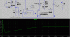
Below is the circuit modified to use a N-MOSFET, which is more readily available. The only difference is that now the positive side is used as the common (ground) reference, but that should not affect you charger since it shouldn't care which side is referenced to common. Just connect the charger polarity as shown in place of the simulated load resistor.

I also changed to a standard 5V zener diode for the voltage reference but the more accurate LT1634-5 I used in the other design will also work.

Edit: Corrected error in schematic.

5V Charger.gif
 
Last edited:
I was going to show Willen how to use a N FET, but I see CR has already done so. Unfortunately, he has forgotten to include any hysteresis in his circuit, and few of the component values are well chosen. Connect the plus input of the 393 through a 1K R and add a 240K R to its output. R2 is to low, a 393 can only sink 15 mA easily, so R2 should be 1K or so. L1 is much too small; with 20 uH the current will increase so rapidly that the comparator will not be able to keep up. 200 to 500 uH will work better. C2 should then be reduced to 47 uF or so. R3 can be 2.2K. I don't know the purpose of R4 and C4, I don't use them when I build this circuit. Converters like this are prone to parasitic oscillation because of negative feedback from stray capacitance .
 
I was going to show Willen how to use a N FET, but I see CR has already done so. Unfortunately, he has forgotten to include any hysteresis in his circuit, and few of the component values are well chosen. Connect the plus input of the 393 through a 1K R and add a 240K R to its output. R2 is to low, a 393 can only sink 15 mA easily, so R2 should be 1K or so. L1 is much too small; with 20 uH the current will increase so rapidly that the comparator will not be able to keep up. 200 to 500 uH will work better. C2 should then be reduced to 47 uF or so. R3 can be 2.2K. I don't know the purpose of R4 and C4, I don't use them when I build this circuit. Converters like this are prone to parasitic oscillation because of negative feedback from stray capacitance .
Below is a simulation of the circuit with the changes you suggested (as I understand them).

My simulation showed that the comparator was fast enough to operate with a 20μH inductor but I increased its value to the minimum you suggested.

I initially didn't include any additional hysteresis because the circuit simulation operates fine without it. But in the actual circuit some added hysteresis may be needed to curb oscillations from any stray feedback between the comparator input and output. That's generally a layout and decoupling issue.

With the added hysteresis and smaller output capacitor, the output ripple is about 450mVpp, which seems rather high as compared to about 50mV for my original circuit. Thus it's not clear that your component values are that well chosen either. I particularly don't understand why you want a smaller output capacitor (?).

R4 and C4 are to damp high frequency oscillations from the inductor and any stray capacitance that can occur when the MOSFET switches off.

5V Charger.gif
 
The sim didn't down load. Your other circuits only work in Spiceland. This configuration is also an unstable linear regulator, so just because it oscillates doesn't mean it is actually working as a SMP. A smaller output cap is supposed to reduce the ripple current in the inductor. I just guessed at 47 uF, but since Spice doesn't agree I won't argue.
 
The sim didn't down load.
I didn't post the sim file, but if you have LTspice I can post it.
Your other circuits only work in Spiceland.
How do you know that?
This configuration is also an unstable linear regulator, so just because it oscillates doesn't mean it is actually working as a SMP.
...........................................
That's a curious statement. It uses a comparator in a bang-bang configuration so it's not linear. And if it's oscillating as intended and generates a regulated voltage why do you suggest it's not actually working? What's your definition of working?
 
I genuinely thought you had left out the necessary parts by mistake, but now it is clear you lack an understanding of the basics of design and I have no desire to waste my time trying to explain it to you. My apologies to Willen.
 
I genuinely thought you had left out the necessary parts by mistake, but now it is clear you lack an understanding of the basics of design and I have no desire to waste my time trying to explain it to you. My apologies to Willen.
That's fine. I also prefer not to waste my time with an arrogant know it all (who obviously doesn't). :rolleyes:
 
Hi,
Sorry, I interrupted, little. I am being puzzle little however. :)

However, I didn't find 34063 chip so my alternative way is to make the DC to DC converter by this comparator and MOSFET anyhow.

Here I following your idea but using my own available parts for easy. Don't worry, will change if got mismatch output by 'real' Device after building it. Here I used 4.7V zener (just to test in Sim) and used one of the comparator by LT (I have LM393 anyway) because I have no library file for LTspice. I used 50N03 N-MOSFET; I have 45N03 (rDS on- 0.02 ohms, 45A) MOSFET in TO-220. I used some standard value resistors for easy. I got nice 4.7V across load resistor as 4.7V ZD reference. There is 3.9KHz ripple exist and ripple amplitude is just 14mV p-p. Increasing the output decouple large capacitor from 270uF to 1000uF, I got less ripple.
 

Attachments

  • DC convertor.GIF
    DC convertor.GIF
    16.3 KB · Views: 397
Capacitor C1 should be connected across D1 to V+ to avoid the large startup-overshoot you are seeing.
 
Hi,
Today measured my cell phone's charging voltage and current and got unexpected result. Nokia genuine adapter (charger power supply) of my simple java phone (Nokia 201) is rated Output= 5V, 450mA. Measurement was--
- Output voltage with no cell phone connected +7.5V.
- Output voltage with cell phone +5.8V charging voltage.
- Battey was almost 20% charged.
- Current was 600mA to cell phone.

Just then I measured another Chinese adaptor--

Rated- 5V, 0.5A
- Output voltage with no cell phone connected +5.6V.
- Output voltage with cell phone +4.7V charging voltage.
- Battey was almost 20% charged on phone.
- Current was 250mA to cell phone.

According to my 1st measurement my cell phone is having 5.8V and 600mA current. So I think 5V input is not critical. Isn't it? It seems very rough arrangement!

Another- how much power and heat will the MOSFET dissipate? I wish not to use heatsink. :) [Going to use '45N03' MOSFET, 30V, rDS (on)= 0.02 ohm, 45A]
 
.................................
Another- how much power and heat will the MOSFET dissipate? I wish not to use heatsink. :) [Going to use '45N03' MOSFET, 30V, rDS (on)= 0.02 ohm, 45A]
The MOSFET should dissipate much less than a watt if in a properly functioning circuit, so no heatsink would be needed.
 
And why your simulation (by LM393) has 80KHz and mine with LT comparator has only 3KHz? Won't it affect to power factor? (I am going to use LM393 in real circuit anyway.) I am not seeing any component related to oscillation speed controll, so feeling amazing:
 
And why your simulation (by LM393) has 80KHz and mine with LT comparator has only 3KHz? Won't it affect to power factor? (I am going to use LM393 in real circuit anyway.) I am not seeing any component related to oscillation speed controll, so feeling amazing:
Post you .asc file for the circuit and I will try to see what the difference is.

P.S. It may be the values of C4 and L1, since that affects the output frequency. Try values of 270uF and 20uH as I used.
 
Last edited:
Hi,
Today measured my cell phone's charging voltage and current and got unexpected result.
According to my 1st measurement my cell phone is having 5.8V and 600mA current. So I think 5V input is not critical. Isn't it? It seems very rough arrangement!
The AC/DC adapter simply powers the charger circuit in the phone. The charger circuit accurately regulates its maximum voltage of 4.20V to the Lithium battery cell and also regulates the maximum current.
If the input voltage to the phone is too low then it will not charge the battery properly. If the input voltage is too high then the charger circuit might over-heat.
 
Thank you AG. Sorry dear Crutschow, I returned to my job (out of home) and .asc was in a computer at home. But you can change the comparator from [comparator] library of LTspice. I used 4.7V zener and also you can get 50N03 mosfet there. Just done!

Do it mean comparator has its internal oscillator here?
 
..............................
Do it mean comparator has its internal oscillator here?
Not if you are referring to the frequency difference between the two simulations. C4 and L1 have a time-constant which is the primary factor determining the oscillation frequency. The on and off of the transistor switch causes a sawtooth type voltage variation on C4. The slope of this sawtooth is determined by the C4-L1 value (larger values mean slower slope) and thus the time for the voltage to go above and below the comparator trigger point, which in turn determines the switching frequency.

Edit: After simulating your circuit I realize the primary reason the switching frequency is lower is because your are using a comparator in the simulation whose response time is too slow. The LT1017 is a slow micropower comparator. You can't arbitrarily interchange a part with something that has significantly different parameters and not expect it to change the circuit performance. :rolleyes: You need one that is at least as fast as the LM339.
 
Last edited:
Ops! You posted a post and few days later edited. I just saw 'alert' for post not for edit, so I almost missed your valuable edited text. I felt like to ask about frequency factor here so opened and saw edited text.

Anyway, OK I got more than 35 pieces of LM393 dual comparator from Dick. I want to know that what might be the difference in performance here between 4KHz (mine) and 80KHz (your)?

I bought some pieces of 5.1v zeners and few others today. I was worrying about TL431 but I found it with cheap rate that I can buy 25 pieces of TL431 by just a dollar. Part is marked as 'LT 33 431NHP' on TO-92 reel package, probably it is from LT company (?)
 
...............................
I want to know that what might be the difference in performance here between 4KHz (mine) and 80KHz (your)?
......................
For a given inductor and output capacitor a lower frequency will give a higher output ripple voltage.
 
Oh I forgot to say-- when I used 1000uF cap and 40uH inductor at output then ripple was small 14mV p-p and frequency was low.

I decreased 1000uF to 270uF and 40uH to 20uH then ripple was large 45mV p-p and frequency was fast.

So I thought that less ripple (14mV) is better with high value caps and L, though it has little slow frequency.

EDIT: I made it too--- :)
 

Attachments

  • DC to DC convertor_built.jpg
    DC to DC convertor_built.jpg
    28.5 KB · Views: 381
Last edited:
But why I am getting 4.6V out from this device (real device I made-shown in previous post)? I used some available resistor and used 100 ohms input R for IC to save IC from high volts like 14 or 15, I think it's not harmful. 5.1V ZD reference input gave me 4.6v output (in load or open load). So thinking to use 5.6V ZD to get around 5V. Anything wrong with the schematic?
 

Attachments

  • DC to DC convertor_built schematic.GIF
    DC to DC convertor_built schematic.GIF
    12.6 KB · Views: 477
Last edited:
Status
Not open for further replies.

New Articles From Microcontroller Tips

Back
Top