Continue to Site

Welcome to our site!

Electro Tech is an online community (with over 170,000 members) who enjoy talking about and building electronic circuits, projects and gadgets. To participate you need to register. Registration is free. Click here to register now.

  • Welcome to our site! Electro Tech is an online community (with over 170,000 members) who enjoy talking about and building electronic circuits, projects and gadgets. To participate you need to register. Registration is free. Click here to register now.

Anyone with experience in microwave (2.45Ghz) design?

Status
Not open for further replies.

Blueteeth

Well-Known Member
Hi,

I've started a new project involving some 2.4Ghz transcievers I got as samples a few years ago - P/N: ML2724. I have a few nordic transcievers, but this is more a project of learning rather than practicality/cost.

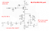
The thing that makes these transcievers interesting/difficult is, they have a balanced RF TX, and a single ended RX side, both with odd impedances. The Tx has two pins, each at 12+j0, open collector outputs. The RX has 2.6-j2.6 input (that seems awfully low to me).

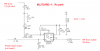
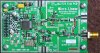
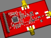
Thankfully I have two reference designs to help me work out whats going on, and whether I can trust the impedance figures given in the datasheet, both designs have full schematics, BOM and gerbers - which I guess I need to look out for transmission lines. As for the Tx, I'm just going straight off the ref design (I can actually get hold of the parts) with matching network -> balun (balanced to unbalanced) then into an antenna switch, no PA, just for short range testing.

But...can anyone help me with an impedance matching circuit for the RX side? The LNA they use is discontinued, and I would like to have a half decent match from a standard 50ohm input (which is what most modern LNA's are internally matched to) to the odd 2.6-J2.6. I realise impedance matching isn't as crucial as many think, but considering I have NO RF testing equipment, I cannot effectively measure what I have made - so I'm trying to get it right first time. This is NOT for 'perfection', purely to increases the chances of it actually working to some degree.

I've been up to my eyeballs in smith charts for the past few days, and despite lots of handy software tools avaliable, experience counts far more :) Frankly, I am out of my depth.

Blueteeth
 
Last edited:
My questions:

- are you planning to make a pcb for this? (I assume you are)
- what reference designs are you working with? I am puzzled because I looked up the reference design for the part that are online at RFMD and the first schematic I brought up (non-PA version) shows an LNA that is a BFG425W and then when I looked up that part on Digikey I find that is indeed available. The design I am looking at is labelled ML2724RD-02_r3p4_sch.pdf.

I understand that this is just a learning exercise, but given that you are going to invest perhaps 50 hours of work and spend more than $30 for materials (perhaps), it seems a bit odd to force yourself to use a particular IC just because you've got a few for free vs spending, say, $5 each for something newer (ie. TRC104 just as the first low cost example I stumbled across at Digikey). Then again, you have to start somewhere I guess.

The schematic shows a fairly simple L match from the LNA collector to the IC input. This is fine. There is nothing fancy being done here, and they don't care about bandwidth of the match because the 2.4GHz ISM band is pretty narrow anyway. So you should be able to plot this on a smith chart and understand it without much trouble. The LNA data sheet provides Smith plots for S11 and S22 to help.

When building at this frequency without any instruments to help you with tuning, you really should copy the eval board (exactly, down to the nearest mm) for the RF signal paths and RF bias.
 
Last edited:
Ron,

Thanks for your reply! I sort of guessed you were an RF guy and was hoping you would respond.

To answer your questions:
- yes, I am making a PCB for this, etching myself with the P&P method. Of course, I cannot get the same tolerances as a board house, but I can now get consistant results for 10/10 mil spacing. I'm using 0603 SMT passives, mainly because of the high frequency but also, for the inductors, thats the biggest size I can get them in :) I've designed with 0603 before, no problem there.

As for the specs of the laminate, it is double sided FR4, 0.032" thickness, 1oz copper. From what I have gatherd from my research into microwave circuits, this is the 'bare mininum' requirment. Not only must there be a ground plane on the bottom side, but also the thickness reduces the width of 50 ohm transmission lines (down to 50mil). However, I am not planning on routing any RF carrying traces more than a few mm, with the possible exception of the antenna trace, to an SMA.

- reference designs. Yes, the one on their site was put on there a few days ago (*possibly* because I asked for a more uptodate ref design). It seems much more extensive than the other one I have, which was sent to me by the original manufacturer, Microlinear, back in 2004. This had no PA, and an RF2472 for the LNA. The Tx side was balance to unbalanced, and using RFsim99, smith 1.91, and Txline (as well as literally writing impedance formulas in Excel) managed to validate it as 'probably going to work'.

Reason for using this particular IC? Well, good point! Many are cheaper, have integrated PA/LNA/Switch, lower power, and generally much 'nicer' to develop with (few components on the RF side). The Chipcon CC2500, and NRF24L01 are prime examples, but those, and it seems all the others have one feature: they control the baseband. The ML2724 is essentially 'dumb' with regard to baseband coding, and packet format, it has DIN, and DOUT, any baseband must be done off chip. With its high datarate, 1.536Mb/s I was interested in using my own channel coding in FPGA's to see if I could possibly get a higher data throughput using these than the nordics (theoretical 1.7MB/sec, tested = 700kb/sec) - that is 'user' through put. It also has the ability to transmit continuously without frequency drift, where-as almost all modern transcievers require either shutdown, or switching to Rx after each packet - further limiting throughput. Another rather stubborn reason is, I have 8 of these left I was given as samples back at university lol, and they are sitting here doing nothing. Its not the best RF chip in the world, but it pushes all my buttons for things like digital audio streaming (one way, but having the option of infrequently transmitting small packets back info about errors etc..)

I asked RFMD for a second reference design (the one you saw) purely because I'm happier having more examples to see what is done, and any common little sub circuits between the two. Also because, with my limited knowledge of RF/microwave (and dare I say, even analogue) the input impedance of the RF input seemed terribly low, at 2.6-j2.6. When I used a smith chart to analyse the matching network, it seems the output of the BF425W based LNA was even lower, at around 1.6+j20.

If I can sort out a matching network for 50 input, I can 'tinker' with external LNA's, the datasheets for which all seem to have nice reference schematics to provide a 50 output imedance. This is opossed to designing a matching network specifically for one LNA.

Apologies for a long winded explaination, if you wish to see the other reference design, I'll upload the PDF in this topic. As 'ghetto' as my design may be, I'm not after ultra low power long range, efficient transmission. Just a couple of tranceiver boards with say 10m range that I can tinker with. I would copy the reference design, but etching my own boards means no plated vias :/ a few of which are under the chip, but I am certainly using as much as I can of it, only changing the LNA and RF switch due to availability. Perhaps I am just being overly cautious here, after all I am only using RFsim99 to simulating matching circuits, and frankly, I don't trust it completely :)

Thanks!

Blueteeth
 
- yes, I am making a PCB for this, etching myself with the P&P method. Of course, I cannot get the same tolerances as a board house, but I can now get consistant results for 10/10 mil spacing. I'm using 0603 SMT passives, mainly because of the high frequency but also, for the inductors, thats the biggest size I can get them in :) I've designed with 0603 before, no problem there

As for the specs of the laminate, it is double sided FR4, 0.032" thickness, 1oz copper. From what I have gatherd from my research into microwave circuits, this is the 'bare mininum' requirment. Not only must there be a ground plane on the bottom side, but also the thickness reduces the width of 50 ohm transmission lines (down to 50mil). However, I am not planning on routing any RF carrying traces more than a few mm, with the possible exception of the antenna trace, to an SMA.
Good choices so far. FR4 will be fine, although even 50thou can be pretty wide when interfacing to small packages. Most parts are designed with hopes of getting into cellphones and the like where 8 to 12 layer boards are the norm, with 4 thou layers and very narrow 50 ohm lines.


Reason for using this particular IC? Well, good point! .....
OK, good enough reasons.

I asked RFMD for a second reference design (the one you saw) purely because I'm happier having more examples to see what is done, and any common little sub circuits between the two. Also because, with my limited knowledge of RF/microwave (and dare I say, even analogue) the input impedance of the RF input seemed terribly low, at 2.6-j2.6. When I used a smith chart to analyse the matching network, it seems the output of the BF425W based LNA was even lower, at around 1.6+j20.
The BFG425W data sheet I looked at showed an output Z of around 70-j35 ohms or so. Did you do that analysis right? I agree that the chip input Z is a bit odd. Its also odd that they say the typical input is 2.6+j0 in the table, then 2.6-j2.6 in the pin descriptions. -j2.6 ohms is the impedance of a 25pF capacitance to ground and I suppose that this is not an outlandish amount for an IC pad.

If I can sort out a matching network for 50 input, I can 'tinker' with external LNA's, the datasheets for which all seem to have nice reference schematics to provide a 50 output imedance. This is opposed to designing a matching network specifically for one LNA.
A good idea, much more modular. An L match from 50 down to 2.6 is in order I guess.

I would copy the reference design, but etching my own boards means no plated vias :/ a few of which are under the chip, but I am certainly using as much as I can of it, only changing the LNA and RF switch due to availability. Perhaps I am just being overly cautious here, after all I am only using RFsim99 to simulating matching circuits, and frankly, I don't trust it completely :)
Sorry but "being overly cautious" and "no plated vias" don't go together in my book, but nonetheless, you might get it to work. Wired vias require more room than good plated through vias, so your ground paths from component to plane will be longer which adds series inductance which is not good (except when grounding an inductor of course).
 
Last edited:
Ron,

Apologies for the late reply, I have been waiting on a few replies to emails I sent out to get more info on the input impedance of the chip - seems I am not the only one who's noticed the error in the datasheet.

You're right on transmission lines to small packages. I have some scrap mini-PCI wifi cards, covered in 0402 passives and DFN chips - I'm guessing the PCB layers must be very thin given the track width to the antenna connector, looks like 16mil. But I am not planning on routing any RF connections more than 2-4mm, anything longer and I will have use 50mil width for the bulk of the line, narrowed down to something thinner when connecting to pins of IC's or the balun (0.5mm spacing). Hopefully the only long trace will be the antenna line. I'll upload a layout here tomorrow.

Btw the -j2.6 is a 25pf capacitance in series, at least by my understanding. The guy from RFMD was kind enough to send me a 'snippet' of yet another schematic they used for development which allegedly is purely a 50ohm transmission line, matched to the RF input. A smith chart shows this matching is waaaay off, but as it was similar to the matching networks in previous reference designs (series inductor, shunt cap, series cap), I'm guessing its the IC's impedance thats 'unknown'.

So, it looks like this is all on hold until I get a ball park figure. I am afraid I am unsure exactly how to work out an 'unknown' load impedance, from a known source impedance and matching network, I have only ever calculated things from the load side. If you know a way to work this out, I would be grateful :) If needs be I'll compile an image of the 3 'example' matching networks - although two of them are matched to two different LNA's, who's output impedance is also unknown. They are pretty basic but make quite pretty wide circles on a smith chart.

Pity, I was all ready to go ahead on this, but no specs, means no finished schematic, which means no PCB, and no 'tinkering'. If anyone is interested, I'll keep this thread updated.

Blueteeth
 
Btw the -j2.6 is a 25pf capacitance in series, at least by my understanding.
Its all a matter of perspective. There is no difference between a series capacitor and a shunt capacitor if the capacitor is the only element in the load. I admit that this is not the case when the impedance is described as 2.6-j2.6, but, to simply make a point that most of the input Z is the terminal capacitance, I was sort of ignoring the 2.6 ohms of resistance since it is quite low.


So, it looks like this is all on hold until I get a ball park figure. I am afraid I am unsure exactly how to work out an 'unknown' load impedance, from a known source impedance and matching network, I have only ever calculated things from the load side. If you know a way to work this out, I would be grateful :) If needs be I'll compile an image of the 3 'example' matching networks - although two of them are matched to two different LNA's, who's output impedance is also unknown. They are pretty basic but make quite pretty wide circles on a smith chart.
Go ahead and compile it. I have a feeling that with all these examples, we should be able to make a good estimate of the chip input Z.

If you want to make some progress, it might be safe to design with a placeholder input matching network that is a pi network of three 0603 chip parts for now and figure out the values later. (if you are ok to work with 0402 parts, use those instead. Smaller is always better at these frequencies. I use a microscope for such work).
 
Last edited:
Hi again Ron,

Here's all the reference designs I have. The tihng they all have in common is they all use series inudctor -> shunt cap -> series cap. I'm guessing its a low pass filter match, but the values are different in every one (probably due to different source impedances used). I may have another rep from RFMD looking into it, although I have made it clear I'm just doing 'research' and not planning on ordering 5k parts, so they probably have more pressing issues.

Although I have used 0402 on several contracts, its really the limit, I can solder 0603's all day but 0402, as you suggested, requires a microscope, so its on the cusp of my 'skills'. Using the utility TXline, it seems if I use a coplanar waveguide (as opposed to just a microstrip) to route the RF, the width can be 32mils. As I'm flooding the top layer with ground plane anyway (as well as the entire underside) seems like a good idea to use CPW, it also makes the RF traces roughly the same width as the pads for 0603. As for non-RF parts, I can easily put a track under 0805, parts, done it a few times on my own boards with 0603 - but never with 0402. Makes layout a hell of a lot easier, allow almost all my via's to be purely ground.

Anyways, I've drawn a blank with all these. If the datasheet is right about the input impedance being 2.2-j0 (or 2.6-j2.6 later on in the document), then although I can design a lovely matching network for this, I cannot reconcile these schematics. My match uses a shunt inductor, and is a fairly wide 'bandpass' - and conveniently uses standard values. These reference ones are totally different on a smith chart.

Regards, and thanks for sticking with me on this :)

Blueteeth.
 

Attachments

  • cid_image002.png
    cid_image002.png
    22.2 KB · Views: 621
  • RXside2LNA.png
    RXside2LNA.png
    32.2 KB · Views: 1,562
  • RXsideLNA.png
    RXsideLNA.png
    15.7 KB · Views: 815
Working backwards from available info I get these values for the input Z of the ic:

for the first image, starting from 50 ohm tx line 9.2-j33 ohms
for the second image, using BFG425W 7.4-j39 ohms
for the third image using RF24xx 3.2-j40

There is a lot of potential error in these estimates because they omit all the pcb contribution to matching impedances, but it is interesting that they are roughly in the same ballpark. Unfortunately, that ballpark doesn't seem to be 2.6-j2.6 ohms. Anyway, this dilemma is one reason why an RF engineer often resorts to using instruments to get the job done.
 
Wow thanks ron!

Using software (due to my lack of experience/knowledge) I resorted to 'randomly guessing' the input impedance and doing the maths for each network to see if it was anywhere near what I thought the source impedance was. I didn't get any consistant results like yours.

You are right of course about instruments. I wish I knew someone who owned a vector network analyzer, who I could buy a pint for. About the PCB traces, I have the gerbers for the second two matches, alas the 'photo's of the boards provided in the two ref designs are not the same, seems they took the snaps of earlier revisions, but the gerbers seem up to date.
Anyway, thankyou so much for taking the time/effort to look into this :) I shall start work on the PCB adding some extra placements for passives in the network, whilst waiting for RFMD to reply. A few weeks down the line, if I am still none-the-wiser, I'll bite the bullet, etch a few boards, and start soldering on certain values to see how it functions (if at all...).

From my calculations, if the matching is off, it doesn't seem to be the end of the world, provided its not WAY off. Given the tolerances of my DIY PCB's, theres a hell of a lot of variance there anyway, so it really will be educated guessing. Its also the RX side, which doesn't seem to be as critical for power transfer as the TX path - which I'm confident is fine in all reference designs, as two schems use 50/50 ohm baluns, so the output really is 50ohm (ish).

Again, thankyou for the figures, gives me something tangible to work with, as well as getting some information from someone who is far more experienced with this sort of thing than I ( = confidence). Even if this all goes tits-up and I end up with dead hardware, I have learned a great deal which is something that keeps life interesting.

Cheers,

Blueteeth
 
I wish I knew someone who owned a vector network analyzer, who I could buy a pint for.
I have one that would be useful, but the logistics of getting your circuit to me and then back again are just a bit too much, I suspect, since I live in Vancouver.

About the PCB traces, I have the gerbers for the second two matches, alas the 'photo's of the boards provided in the two ref designs are not the same, seems they took the snaps of earlier revisions, but the gerbers seem up to date.
Can I assume that you are using a gerber viewer to look at those?


Anyway, thankyou so much for taking the time/effort to look into this :) I shall start work on the PCB adding some extra placements for passives in the network, whilst waiting for RFMD to reply. A few weeks down the line, if I am still none-the-wiser, I'll bite the bullet, etch a few boards, and start soldering on certain values to see how it functions (if at all...).
its perfectly reasonable to guess that you will need an L or Pi topology for the matching and so just place three parts in pi configuration and then later do some educated guesswork and trial-and-error. Soldering parts on and off to optimize a tune is standard procedure in this business (but usually we start very close).

If I assume the input Z to be, say, 8-j39, it is easy to get there from 50 ohms with two components. I only hope that you do everything you can to keep traces short, pads small and so on.

You mentioned co-planar before and thats fine, but you really should stitch the top layer ground plane to the lower ground plane at numerous places, and since you are using wire vias, that is going to be fair bit of work.
 
I have one that would be useful, but the logistics of getting your circuit to me and then back again are just a bit too much, I suspect, since I live in Vancouver.

Good point, but thankyou if that was an offer :) Of course not doubt it will either work partially or perhaps quite well, but if I'm reeeeally stuck, I may ask if I can ship you a board. No point in returning it though, I'll know the layout and component values anyway for a tweak on the next version. Got 8 of these chips, just want two boards to tinker with.

Can I assume that you are using a gerber viewer to look at those?

Used 'Gerbmagic'. One ref design is double sided 0.032", the newest on their site is a four layer with the bottom and second from top being almost all ground plane. That would explain why the transmission lines are so thin on that one. But on the thinner board (double sided), I measured the transmission line widths as exactly 30mil, although there is ground plane on the top too, so perhaps its coplanar. I'll add a photo of it tomorrow, its alot more compact and dare I say 'slack' with regard to RF routing. With only a few traces designed for RF, as well as a 'post build' modification of a PCB trace antenna, looks like it was cut with a knife - I guess thats standard practice as well, for tuning.

If I assume the input Z to be, say, 8-j39, it is easy to get there from 50 ohms with two components. I only hope that you do everything you can to keep traces short, pads small and so on.

For both RF/impedance efficacy, I'm trying to keep SMT parts as close as possible, making it a bit harder to populate, but I'm certainly not going to space everything out. However, my idea was to keep the matches very close the the chip, tightly grouped, and have two transmission lines going out, Tx, and Rx. These would then extend to SMA's on opposite sides of the board.

Now, this may not be good design practice, but I was hoping to use 0ohm resistors as jumpers to select between these transmission lines going straight off to SMA's, or onto other transmission lines, which would go to a PA, LNA, and a switch, which then gets sent out (via another transmission line) to a third SMA. That way I have direct access to 50 ohm matches, with seperate Rx and Tx connections for debugging, but the option of attempting to use a 'front end'. The IC's for which I have robbed from a PCI-mini wifi card.

**broken link removed** - LNA
AWL6950 datasheet pdf datenblatt - ANADIGICS, Inc - 2.4/5 GHz 802.11a/b/g WLAN Power Amplifier ::: ALLDATASHEET ::: - PA.

They're dual band, but if I power down the 5.8Ghz side on both, they seem a bit too good to be true, even though they're DFN. 50ohm in/out and decoupling, that's it. Perhaps I should make separate tiny boards for these and use SMA cables though.

You mentioned co-planar before and thats fine, but you really should stitch the top layer ground plane to the lower ground plane at numerous places, and since you are using wire vias, that is going to be fair bit of work.

Yeah, can't say I'm looking forward to it. My last double sided board had 18 via's which wasn't fun either, and this design will require via's regularly spaces along each transmission line, as well as generously spread across the entire board - just for GND. My half arsed method is to drill 0.55mm/0.6mm holes, use 0.6mm single core wire wedge in, and cut then excess with a semi blunt pair of wire cutters. Then, I put the whole thing in a vice to 'squish' down the tiny bit of wire protruding out of each side. Solder each one to make a nice small 1mm 'dome'. Neat and functional, and its surprisingly quick. I know I know, I've really made life difficult for myself with this project eh?

Who knows, if customers start paying up early, I might get cheat and get boards made up. Still two layer though (can't afford 4 layers) but it would certainly make it much more likely to function properly.

Again, thankyou, and apologies for such long descriptions, I could of course flood the topic with pictures, gerbers, schems n all that, because they are much better at showing idea's, but I don't wanna use up too many forum resources :) So I'm using em sparingly. If you're really interested in this as a problem, I'll be happy to PM/email you all I have in a zip file.

Scott.
 
Update!

First of apologies for such a long drawn out reply above... I used the quick reply function and didn't realized just how big and 'full of waffle' it was. You have probably gathered I can talk for England eh

Yet another guy at RFMD has proven very helpful, sending me a full reference design that was the original (and final) starter kit used to show off the transceivers capabilities. This has the first 'match' in my previous post (5pf, 3pf shunt, 1nH) directly to a 50 ohm line. They also did what I was planning on doing, and using 0ohm jumpers to select between direct 50ohm SMA, and a PA/LAN front end. So thats a bonus! Full gerbers, BOM, and specs were provided.

With no less than three FULL reference designs, including one which I'm confident is proven (the starter kit) I'm starting the PCB right now, along with your recommendation of a pi network footprint added for tinkering. I've included a photo of starter kit board, which I am basing mine on, with some less features, and a different front end. There's enough via's on there to make my dremel weep, but a 0.8mm(32mil) board is a lot nicer to drill, than standard 1.6mm.

Thankyou once again for your advice/knowledge and recommendations on this Ron. Couldn't have slogged through it all without you. Now the 'planning' stage is almost done, so begins layout, PCB manufacture, and all that other stuff which breaks my spirit.

Cheers!

Blueteeth
 

Attachments

  • rf_board.jpg
    rf_board.jpg
    737.9 KB · Views: 1,436
Last edited:
Update!

Well, it has been a couple of months, but I haven't forgotten about this project (or Radiorons help!).

I ordered a batch of parts last month, but still need a few more passives... as I got used to using smith charts and other software to work out optimum values for caps and inductors, as well as managing to get hold off some half decent RF amps.

Here's the layout so far. Not complete, still requires the logic for the TX/RX switch, an oscillator, and a regulator. But I'm satisfied with the RF, as much as I can be. I realise without studying the datasheet for the transceiver or any of the parts, one can't give much in the way of specific advice on the PCB - but I would appreciate some constructive crticism on it. Its my first microwave/RF PCB, and I've probably been overly cautious, but its still within the limit of my PCB making/soldering.

Cheers!

Blueteeth
 

Attachments

  • ML2724RD3Ea.png
    ML2724RD3Ea.png
    185.6 KB · Views: 987
It looks pretty good, so my list of quibbles is not long.

At these frequencies I would avoid thermal reliefs on ground pads.
It appears that your SMA connector leads do not land on your SMA ground pads.
I would include some additional ground via stitching along the tx lines leading to the connectors.
You need to stitch the edge of the board with ground vias. The edges are where current tends to collect and they have to be taken to a common ground.
I usually back my ground away from the tx line a bit more than you do, but if you are calculating your line width by accounting for the contribution of microstrip and coplanar impedance, then it is fine.
I'm not sure about this point, but it seems as though your center lead pad on the SMA connectors is wider than it needs to be. Why are you using that particular width?

Not an "error" but:
when I'm making a prototype, I often try to predict where I may have to add shunt components for matching or whatever and leave the ground plane alongside the signal trace without a solder resist covering so that i don't need to scratch it off to play with adding parts.
 
Last edited:
Status
Not open for further replies.

Latest threads

New Articles From Microcontroller Tips

Back
Top