Continue to Site

Welcome to our site!

Electro Tech is an online community (with over 170,000 members) who enjoy talking about and building electronic circuits, projects and gadgets. To participate you need to register. Registration is free. Click here to register now.

  • Welcome to our site! Electro Tech is an online community (with over 170,000 members) who enjoy talking about and building electronic circuits, projects and gadgets. To participate you need to register. Registration is free. Click here to register now.

Analysing Power Amplifier circuits-General discussion

Status
Not open for further replies.
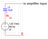
If R10 carries the emitter current for Q7 there will always be a DC input offset. 10k from node 14 to ground would set the emitter current of Q7 to 2.5mA, eliminating offset voltage.

It's not a spilt supply amplifier, with a DC coupled output, so a little offset isn't a problem - you don't add an axtra resistor on these designs, there's no need for it. What you do is design the front end potential divider correctly, and not just half and half as it is now, in order to give the maximum possible output voltage before clipping - some designs even include a preset so you can tweak it.
 
just clarifying........does the positive terminal of the capacitors all face ground whils the negative terminal of the capacitor faces the negative supply rail?
 
just clarifying........does the positive terminal of the capacitors all face ground whils the negative terminal of the capacitor faces the negative supply rail?
Mostly. Simply look at the voltages at each wire of each capacitor.
 
in the last circuit diagram i posted of the power amp im building,

THE VOLTAGE SOURCE (V1) TERMINALS are the wrong way around?

the positive terminal of V1 should go to gnd?
 
What?
Why are you feeding a signal as high as 120VAC to the input of the amplifier?
It will blow it to kingdom come.
The input to the amplifier is AC, not DC and is about 0.07V, not 120V.

The 120VAC connects to the primary of a power transformer. The 36VAC secondary of the power transformer connects to a bridge rectifier then to a big filter capacitor to produce -50VDC.
 
V1 is an AC source. it doesn't matter much. if you reverse the terminals, you still get the same waveform, voltage and current, but with a phase inversion, which might matter some in a circuit sim.

another note about running this in a sim, or troubleshooting with an oscope.... troubleshooting the circuit may prove to be a bit "counter-intuitive", in the sense of what happens in the "top" half of the amp will be seen in the bottom (negative) half of the waveform on an oscilloscope (or sim) and vice versa. it's not a real problem once you get used to seeing it that way. with the sim you can set the scaling reversed if you wish, and some oscopes have an invert function if you wish to use it. so just keep in mind, when you see the waveform "hanging" on the negative peak during clipping, it's the bottom transistor that's saturating.

audioguru wrote:
No.
You want node 14 to be close to the DC output voltage for it to be biased at half the supply voltage. The emitter current for Q7 is in the feedback resistor R10.

you're right.... it's been about 20 years since i've troubleshot an amp of this type... a Dynaco Stereo 40 if i remember correctly.....
 
I am not feeding a signal as high as 120VAC to the input of the amplifier. I said before, ignore details on voltage source 1, but you are forgiven:D you read alot of threads a day & must have forgotten

What?
Why are you feeding a signal as high as 120VAC to the input of the amplifier?
It will blow it to kingdom come.
The input to the amplifier is AC, not DC and is about 0.07V, not 120V.

The 120VAC connects to the primary of a power transformer. The 36VAC secondary of the power transformer connects to a bridge rectifier then to a big filter capacitor to produce -50VDC.

fantabulous68

-50V Single negative supply- 8 ohm load- single transistor input
Done "normalizing";

Fixed the connection from the emitter of Q7 to ground that was shorting it out.

Hope its fine now

ignore details on V1 (AC voltage source)
 
GrrrrrrrrrrEaT News!!!!!!!!!!!!!
i changed the amp a little BUT BUT BUT it worked:D

Im going to take pics tomorrow and upload it here:)

I was real excited when it worked lol.

"KILLED" some transistors along the way because I didn't check if i was given the exact transistor I asked for.
:)

I will also upload the circuit i used and worked.

I learnt alot & had alota fun

as a friend of mine who is a construction framer always says "measure twice, cut once".... always double-check your parts when building or repairing.
 
I said before, ignore details on voltage source 1, but you are forgiven
You have been posting unattributed, inaccurate, and incomplete schematics throughout this thread, expecting us to refer back and forth while reading your mind and trying to distinguish between transcription errors, design errors, and tricks.

I'm glad that you are quick to forgive when one of your volunteer tutors fails to be perfect.
 
I am not feeding a signal as high as 120VAC to the input of the amplifier.
It is clearly shown on your schematic that is covered with Chicken-Pox dots.
 

Attachments

  • analysing power &#97.PNG
    analysing power &#97.PNG
    2.8 KB · Views: 291
you want that input transistor regular or extra crispy?

must have been a severely clipped output when he simmed it.....:confused:

i've heard of speakers that can withstand being directly plugged into the wall outlet, but never an input stage to an amp....:eek:
 
It is clearly shown on your schematic that is covered with Chicken-Pox dots.


What is also shown is what i said previously..............IGNORE DETAILS OF VOLTAGE SOURCE V1.
 
Last edited:
Results

The circuit was now tested with the load and had the following settings:
Frequency =1.5 KHz.
Input signal was set at 50mV/DIV for pic 1 ---->100mVp-p
Output signal was set at 1V/DIV for pic 1---->3Vp-p
The input signal is the top waveform. The output signal is the lower waveform.

The signal at the output had an amplitude of 3Vp-p. The gain was calculated to be 30V/V while the predicted value was 30V/V.

--------------------------------------------------------------------------------------------------------------------
The input signal was then varied from 10 kHz to 20 kHz. The amplitude of the output waveform decreased. The gain also decreased as the frequency was varied from 10Hz to 20 KHz. Hardly any distortion was seen.

At 10 KHz the following output was observed on PIC2:
At 10 KHz the amplitude of the output waveform was 2Vpk-pk. The gain was 20V/V.


At 20 KHz the following output was observed on PIC 3:
At 20 KHz the amplitude of the output waveform was 1.2Vpk-pk. The gain was 12V/V.

More results to come(class B crossover distortion etc:D)

Please feel free to comment on the oscilloscope results :).
 

Attachments

  • 1..PNG
    1..PNG
    218.6 KB · Views: 304
  • 2..PNG
    2..PNG
    231.7 KB · Views: 319
  • 3..PNG
    3..PNG
    177.9 KB · Views: 288
Last edited:
PIC 4

To observe a class B output on the oscilloscope, the Vbe multiplier transistor was shorted out between its collector and emitter. The circuit was now tested without a Vbe Multiplier and the oscilloscope had the same settings as before.

Crossover distortion was viewed on a scope in the form of a ‘kink’ in the output curve as seen above. This is a characteristic of class B Mode.
When the circuit was tested with a Vbe multiplier and the potentiometer was adjusted, the output curve smoothed. By adjusting the potentiometer in the VBE multiplier, the base bias voltage VBB is changed. This changes the quiescent current that flows. By adjusting the quiescent current, the class of the amplifier changed. β is not exactly known, so there is no way to choose specific resistors to bias the transistors for a certain class. Therefore a potentiometer was used.

Any clue why the input signal is distorted? Does it have to do with feedback and slew rate?

PIC 5

The next test was to measure the total harmonic distortion (THD) of the amplifier. Total harmonic distortion is measured in percentage terms and is a representation of the distortion of an audio signal at full output level. A clean sine was required to be inputted into the circuit. A function generator will not be able to generate a clean sine wave therefore a spectrum analyzer used. The input sine wave was set to a fundamental frequency of 1.5 kHz & 25mVpk. Thereafter harmonic markers were placed on the signal. The THD function that the spectrum analyzer had was implemented. The THD measured was 0% as seen in the figure below. This was an acceptable value since no distortion was visible on the output waveform. THD should be around 0.01-0.1%.
 

Attachments

  • 4..PNG
    4..PNG
    259.6 KB · Views: 299
  • 5..PNG
    5..PNG
    535.9 KB · Views: 303
Last edited:
2 & 3 are rather distorted - if you can see it on a scope it's really bad.

Is it distorted more at higher(20KHz) or lower frequencies(10KHz)?
I would say 20KHz since the gain lowered, right?
I should put my glasses on
 
Last edited:
Status
Not open for further replies.

Latest threads

New Articles From Microcontroller Tips

Back
Top