Continue to Site

Welcome to our site!

Electro Tech is an online community (with over 170,000 members) who enjoy talking about and building electronic circuits, projects and gadgets. To participate you need to register. Registration is free. Click here to register now.

  • Welcome to our site! Electro Tech is an online community (with over 170,000 members) who enjoy talking about and building electronic circuits, projects and gadgets. To participate you need to register. Registration is free. Click here to register now.

Analysing Power Amplifier circuits-General discussion

Status
Not open for further replies.
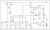
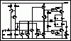
Power Amplifier circuit 2

how do i delete this?my msg got duplicated, my net was slow & i clicked send twice.....Sorry....I cant find the delete icon
 
Last edited:
In your new schematic, The input bias resistors R12 and R13 need an RC filter to prevent hum on the supply from being amplified.
R11 can be replaced by current mirrors and R14 can be replaced by a constant current sink.

C3 provides "bootstrapping" for R7 and R8 so that when the output goes low then the voltage across C3 drives the junction of R7 and R8 to below 0V so that Q5 still has enough base current to saturate well.

It is all described in the Guitar Amplifier document.
 
Yeah thanks Audioguru, Im going to try downloading that document again now. My net did not download it when i tried yesterday....it was taking forever.....


What do R6 and C1 do?

I tried twice to download it...it gave me the same error msg:


Foxit Reader: Format error: not a PDF or corrupted.....
 
Last edited:
R6 and C1 in your power amplifier produce "frequency compensation". They reduce the gain at high frequencies so that at a frequency where the phase shift converts negative feedback into positive feedback then the ampllifier's gain is less than 1 so it does not oscillate. All opamps have similar frequency compensation.
R9 and R10 provide negative feedback.
 
The new circuit still depends on luck to avoid thermal runaway.
No.
If the Vbe multiplier transistor is bolted to the heatsink where the driver transistors are mounted then its voltage decreases as it warms so it cancels thermal runaway.
 
Yes, if the builder is lucky he would choose the right Q2 to match the temperature coefficient of the output stage. And if he's even luckier the values of R4 and R5 will be right the first time.

If he is lucky he will also notice that R2 is shorted.
 
I wouldn't be too worried. Q2 is typically a low power type with a high temperature coefficient. It doesn't really need to match; it only has have a higher coefficient. Also, the gain is stabilized with closed loop feedback. If the output tries to runaway, the loop will pull it back.
 
Last edited:
still no emitter resistors in the output stage... a recipe for disaster....

i don't like it when the centerline (speaker terminal) is brought back to the driver stage. if one of the outputs short, it's more likely to cause a chain reaction self destruct all the way back to the input stage. yes, when designing any circuit, you have to remember it may at some point need repair. i don't think the OP is familiar with current sources and current mirrors. the original design posted had a very low tail current in the diff amp section (30V/330k=90uA) so not a whole lot of open loop gain. if you want to study up on a crash course in amp design, look here:
**broken link removed**
that will get you started at least. there's a lot more than picking a bunch of pieces and putting them together. there's a logical thought process involved, much like playing chess...
 
Last edited:
New power Amplifier Circuit

The circuit (in the attached diagram) has a Complex O/P configuration and Trans-resistance amp

I welcome any views on the circuit.
 

Attachments

  • ampcct6..gif
    ampcct6..gif
    6.3 KB · Views: 317
It is the strangest amplifier that I have ever seen.
I see nothing that sets the output (before the output coupling capacitor) at half the supply voltage.
It does not have a frequency compensation capacitor.
 
Looks rubbish to me?, and still VERY badly drawn, with no idication of which wires join and which don't.

Which to be honest has annoyed me because I showed him how to show connecting vs crossing but non-connecting wires before and he didn't pay attention.
 
where to begin...

where did you find this one?

first a few comments on the output stage, because no matter how you get there, output stages are all very much alike.

1, why the diodes across the emitter resistors? not really necessary
2. Q10 and Q11 should have about a 100 ohm resistor between them. if you don't provide a discharge path for the capacitance Ccb of Q14 and Q15, the clipping behavior will be terrible.
3. the bias transistor Q8 would be better off with a 10uf or so cap across the C-E junction. you want a DC bias between the driver bases, but the same AC signal on the bases.
4. any particular reason for the driver stage to be composite transistors? it's not really necessary.
5. put "kickback" diodes across the C-E junctions of the output devices to protect them from inductive spikes. these would be 1N4004 diodes with the cathode towards the positive rail.
6. add a zobel network (a 10nf cap and 10 ohm resistor in series) from the output to ground, and a 25uH coil in parallel with a 10 ohm resistor between the output terminal and the load. the zobel network shunts any RF or high frequency oscillation to ground. the coil and resistor isolates any speaker capacitance from the amp and helps prevent oscillation.

comments on the VAS (Voltage Amplifier Stage)
1. why the complicated current mirror and current source setup? it will work, but a simple current source as the VAS load would be simpler, and just as effective.

Input stage:
1. why the nonlinear feedback through Q3 and the diode connected Q4? part of the reason for negative feedback is to reduce distortion. it would be better to add an emitter resistor to Q5 and apply the negative feedback at the emitter. (again, look at the design for a Dynaco)
2. although they were sucessful through the late '60s into the late '70s, single ended input stages have some problems, one (PSRR) is mentioned below as part of a more general question,. another is the tendency towards even harmonic distortion because it is a single ended circuit with no effective cancellation of the transistor's nonlinearities.
there may be more, but i'll post them as i think of them...

another question in general... why the single ended design? a lot of good amps were single ended, like the Dynaco, but they suffered from poor PSRR (Power Supply Rejection Ratio) and required EXTREME filtering of the power supply rails the development of diff amps was a huge implrovement, and also simplified the negative feedback
 
Looks rubbish to me?, and still VERY badly drawn, with no idication of which wires join and which don't.

i know what you mean, somebody came up with this method of drawing schematics back in the '70s, and it takes a bit of getting used to. the basic idea is lines that just cross are not connected, lines that come to a "T" are connected. it's great for drawing freehand, but is terrible of you're looking at a photocopy or a very complex schematic.
 
It is the strangest amplifier that I have ever seen.
I see nothing that sets the output (before the output coupling capacitor) at half the supply voltage.
It does not have a frequency compensation capacitor.

i think the direct coupled negative feedback was intended to take care of the DC centering problem. but it's very poorly implemented feedback. the lack of a compensation cap is tjust icing on the cake...
 
Looks rubbish to me?, and still VERY badly drawn, with no idication of which wires join and which don't.
.

Which to be honest has annoyed me because I showed him how to show connecting vs crossing but non-connecting wires before and he didn't pay attention.

Guys i did not design the circuit. I wasn't even born in the 70's;).

What does the circuit Q1-2 achieve? and where is the path of the feedback system?
 
Guys i did not design the circuit. I wasn't even born in the 70's;).

What does the circuit Q1-2 achieve? and where is the path of the feedback system?

Like your previous circuit, it doesn't look like a complete working design, and this one even less so.

And like we've repeatedly told you, draw the circuits properly, identifying joins and crossovers.
 
Hero999 & Nigel................Hope you'll pleased with the appearance of the cct now....


Getting back to the electronics....
What does the circuit Q1-2 achieve? and where is the path of the feedback system?
 

Attachments

  • ampcct66..GIF
    ampcct66..GIF
    7.3 KB · Views: 319
Last edited:
Hero999 & Nigel................Hope you'll pleased with the appearance of the cct now....

Getting back to the electronics....
What does the circuit Q1-2 achieve? and where is the path of the feedback system?

It's drawn better now - but it's still non-functional, nothing like a working amplifier, and nothing like the 70's either.
 
Status
Not open for further replies.

Latest threads

New Articles From Microcontroller Tips

Back
Top