Alex_rcpilot
Member
Altium Designer - unknown marker found on PCB track
Hi guys, I ran into this problem as I was finishing up a project with Altium Designer Build 9.3.1.19182 that our company has recently purchased.
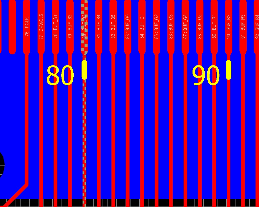
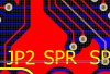
If you take a look at the screenshots below, you'll find out that one of those tracks has checkered flag patterns all over it. Never noticed when it got there though. My first thought was it could be some type of error. So I ran DRC but the results came out clean.
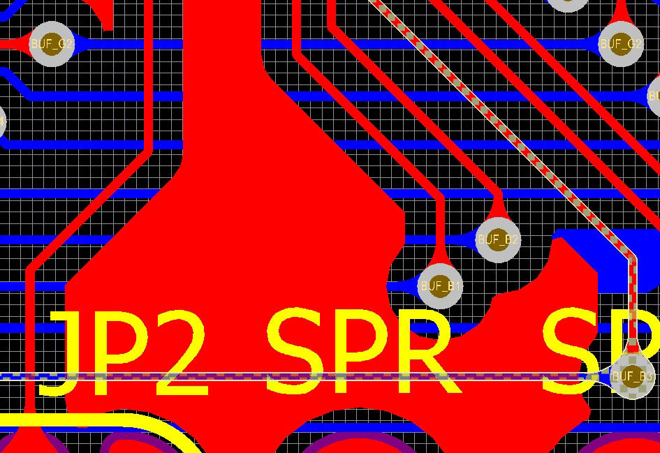
Then a friend said it could mean explosed copper. Since I'm the one who drew this board, and I couldn't recall implementing any special treatment to this pice of wire unlike the rest, I found that hard to believe. So I switched to 3D preview mode, there was indeed no exposed copper wire.
Then I brought up the netlist manager, manually deleted Net BUF_B3, and this marker disappeared. I updated the project to recover the net afterwards, the net came back, but the marker was no longer seen anywhere.
I'm really curious about what it might have been, but I couldn't find appropriate key words to search for official explaination regarding this type of marker. Has anybody got an idea of what it meant? Thanks.
Regards,
Alex
Hi guys, I ran into this problem as I was finishing up a project with Altium Designer Build 9.3.1.19182 that our company has recently purchased.
If you take a look at the screenshots below, you'll find out that one of those tracks has checkered flag patterns all over it. Never noticed when it got there though. My first thought was it could be some type of error. So I ran DRC but the results came out clean.
Then a friend said it could mean explosed copper. Since I'm the one who drew this board, and I couldn't recall implementing any special treatment to this pice of wire unlike the rest, I found that hard to believe. So I switched to 3D preview mode, there was indeed no exposed copper wire.
Then I brought up the netlist manager, manually deleted Net BUF_B3, and this marker disappeared. I updated the project to recover the net afterwards, the net came back, but the marker was no longer seen anywhere.
I'm really curious about what it might have been, but I couldn't find appropriate key words to search for official explaination regarding this type of marker. Has anybody got an idea of what it meant? Thanks.
Regards,
Alex
Attachments

Last edited:
