Continue to Site

Welcome to our site!

Electro Tech is an online community (with over 170,000 members) who enjoy talking about and building electronic circuits, projects and gadgets. To participate you need to register. Registration is free. Click here to register now.

  • Welcome to our site! Electro Tech is an online community (with over 170,000 members) who enjoy talking about and building electronic circuits, projects and gadgets. To participate you need to register. Registration is free. Click here to register now.

A tiny PCB

Status
Not open for further replies.

Boncuk

New Member
Hi,

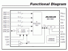
when studying data sheets of GPS receiver modules I stumbled over a voltage regulator in a SON-6 package, the (TI) TPS62231, a 1.8V/max 500mA stepdown regulator.

It's dimensions are 1.5X1mm.

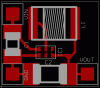
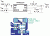
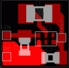
Here are the schematic and PCB design. The PCB measures 7.4X6.5mm.

Boncuk
 

Attachments

  • 1,8V-SUPPLY-SCH.gif
    1,8V-SUPPLY-SCH.gif
    7.7 KB · Views: 436
  • 1,8V-SUPPLY-BRD.gif
    1,8V-SUPPLY-BRD.gif
    11 KB · Views: 463
That's pretty damn small. At my work we have a small GPS receiver board for some kind of PDA - it didn't work, but it never got returned; some of the SMD parts on that thing look like they fall well under 1mm pitch/width (I'm not even sure what the parts are - two terminal, so likely diode/cap/resistor or similar). I tend to wonder if hobbyists will ever get down to that level - probably not making a board completely by hand, but perhaps by some sort of robotic microscope pick-n-place system (if not completely automated). I mean, at one time it was thought that SMT was going to be the death of hobbyist electronics, but it hasn't seemed to stop anyone yet. I just wonder what's coming down the pipe...
 
Coming down the pipe

Hi Cr0sh,

it has already come down. :)

Here is a chip which will cause nightmares trying to manually solder it into place.

It's a MAX19681, a DAC with 4 (channels) of multiplexed 12-bit LVDS (low voltage differential signal) inputs at 375MHz.

It comes in a 169-pin CSBGA (compact size ball grid array) package. Chip dimensions are 11X11mm. :D

Boncuk
 

Attachments

  • MAX19681.gif
    MAX19681.gif
    42.3 KB · Views: 378
  • MAX19681-FD.gif
    MAX19681-FD.gif
    29.7 KB · Views: 420
Last edited:
Oh - geez - that's insane, Boncuk - as if BGA wasn't already a near nightmare for hobbyists (if they dared to use them - I know there a crazy dudes out there into reflowing BGA packages like on a XBOX). I really wonder what we'll see hobbyist-wise as things progress. I wouldn't be a bit surprised if everything goes virtual, and you have to ship designs out and get them fabbed really cheap - pcb, soldering, etc - its close to that today, almost. Perhaps we'll see desktop PCB printers of some sort! Crazy...
 
Hi cr0sh,

I really hope semiconductor manufacturers see the fact that there are millions of hobby electronics freaks all over the world, not wanting to be bothered to purchase an SMD soldering oven, pick'n place machines and all the machinery necessary to "fabricate" a "professional" PCB suiting their (chip manufacturing) requirements.

ATMEL and MICROCHIP obviously know about the problem more than other manufacturers do.

They offer their chips SMD and DIP based.

Regards

Boncuk
 
Nice looking board, Boncuk! I hate working with micro-tiny parts like that though. I especially hate DFN/QFN packages.

@cr0sh - I reflowed a BGA video chip on a laptop MB for a friend of mine at work the other day using a small Weller heat gun. We figured that since the laptop was a freebie and it didn't work anyway, we didn't have much to lose. He says it works fine now. Score!

Speaking of BGA soldering, has anyone ever used the "Stencilquik" product? They look as if they would be easy to use, but I haven't needed to use BGA's in any of my designs yet. (trying to stay away from that)

Here's a link: Stencilquik
 
I've got a kit coming up and sourcing parts large enough to be hand soldered isn't easy anymore. The 100pin TQFP PIC is tricky enough and as mentioned some companies like Maxim don't even make the larger packages on their newest devices.

I was considering a simple clampdown system for holding the 100pin TQFP in place to aid soldering. Although I haven't tried it four round holes at the corners of the IC and four machine screws and nuts as a simple clamp while to hold the IC before you tack it down.
 
Not too bad for the first time, is it? :D
Your layouts are always excellent.

--

I would rather use a QFP than a dip or anything through hole. I'd rather use a QFN than a QFP. They aren't hard and I have trouble understanding how a 100pin QFP is harder than a 32pin QFP. You have to align both the same. If anything the 100pin QFP is easier since it's bigger. Tin a pad at the corners and tack it down. Everybody I've heard talk about moving to SMD full time could never go back to PDIPs and I cringe when I have to put a hole in a board, even if I don't have to drill it myself.

I have to use 0402's for a project that's coming up and I'm thinking of moving a lot of my resistors to 0402's.
 
What I tend to wonder about, and being ignorant of the industrial techniques of electronics - is how new designs are created? I mean, they don't likely breadboard everything; in fact, for some designs - especially things like PC motherboards - this would be impossible. Even for smaller designs, where most SMT components must be sourced (since many aren't available in DIP), breadboarding would be difficult or impossible as well (I know that there exist chip adaptors and such for some SMT packages).

So how is that "first" prototype made? Is it entirely done on a computer, with circuit/component simulation software (SPICE and the like), gradually transfered from a schematic and simulation to a PCB layout, then a prototype PCB fabricated, bugs worked out (and back thru the cycle), then final design implemented?

If parts continue to become unavailable in DIP form (as they seem likely to be), such an above cycle would be very expensive and time consuming for just trying out an idea by a hobbyist. Circuit simulation software (of the level I would imagine needed for, let's say, creating a complex SMT-based ATMega1280 with KS0108 GLCD embedded system of some sort - maybe like a pocket oscilloscope, for instance) wouldn't be cheap (and for instance, in my case, would likely only run on Windows, thus necessitating me purchasing a Windows license on top of everything, increasing the cost), then there's the PCB creation, parts placement, reflow - then you find a problem that can only be fixed by starting over (and you are likely out money in the meantime, depending on whether you can save any of the components from your first cycle).

Is this what we are likely to look forward to in the future as hobbyists: A hobby only the rich (and extremely dedicated) can afford? Electronics is already a fairly expensive hobby (maybe not for most components, but you add up the costs for tools, time to learn software, storage costs, etc - its not small change); are we likely to see it grow beyond what a beginner could afford...? What about a small business - will it become unaffordable for even a small company to implement designs in the future?

I know I must be missing something...
 
There arer a few problems with the layout, remember this is a 2 MHz switching converter, all parasitics are critical...

- IC1 should be closer to C1
- Traces should be thicker
- GND should be a copper pour (same for input, output, and SW) or at least thick traces
- board area could be halved by placing the inductor on the other side
- feedback is not taken from the proper point (after C2, not before C2)
- unshielded inductor will radiate
- no ferrite bead on input, so input wire will radiate
- no ferrite bead on output, so output wire will radiate

Sorry ;)
 
I know I must be missing something...

Ya, I think you are. It definitely has a higher learning curve to get over the initial hurdle of using SMD components and doing PCB design, but many companies now sell breakout boards for SMD components and even modules. Using an ECAD program tends to take a lot of the user errors out of the prototyping process. People tend to think that because they have to remember what every physical pin is in order to point to point it on a breadboard, it's going to be that much harder when making a PCB, but with an ECAD, as long as your footprints are all correct, the schematic takes care of all of this for you. If you absolutely don't want to etch your own boards, there are many 1 board PCB services now, like BatchPcB, Dorkbot PDX, and Itead Studio that are not expensive.

I see SMD as being a boon to small production runs. You can see small production video's, like when they are making conference badges. Run PCB through a stencil with paste, someone drops the components on top, next person puts it on a hot plate, check for bridges, done. With through hole components and soldering, this would be impossible to do in any where near the time or the cost. Small businesses like Adafruit can get a pick and place that is significantly cheaper than trying to do the same thing with through hole components.

I can't believe there's still concern over the move to SMD.

It isn't that I have a concern with EDA (ok, for me, I haven't done much with it, because I have yet to have a need for it - but I imagine that when I do, I plan to dive in head first, likely using gEDA and/or the kicad suite of tools, since I run *nix); my question is more along the lines of how a design can be built and tested, cheaply (for the hobbyist), in the way a thru-hole design can. You certainly can't (without spending a bit of money on many breakout boards) quickly roll an idea up like you can with DIP parts, using "rules of thumb" (and later go back and make modifications as needed based on real numbers).

I understand that yes, once you have a finalized and working design, building it using SMT can be easily done; the question is how you get to that point without spending way more money than you would breadboarding and perfboarding a circuit. Furthermore, what -if- you wanted to just breadboard a single design, then transfer it to perfboard? Today, you can do this somewhat easily, even with SMT components; but what about the future? Are we all going to have to buy a ton of breakout boards, just to try things out? What if you can't use such boards or even perfboard/breadboard construction because of frequency restrictions (to an extent, this applies today)? How do you build a prototype circuit in SMT, without going through the entire design process, spending a not-so-small chunk of money on getting boards developed - then finding your boards were completely wrong?

Versus using thru-hole components on a breadboard, where you can easily move around components and such at will, without needing a new board each time (even with a perfboard, you can do this to an extent - or you just get another perfboard).

Now - I know there are many prototyping PCBs for SMT work; but even there, they aren't super cheap, and if you mess up royally, you may have lost those components and the time, effort and money of the board. You can just remove the components from the board (or from a breadboard), and try again...

Once again - how is an SMT prototype built in the industry? Can anybody point me to something that explains and lays out all the steps, going from an idea through to the finished product? Finally, is this process fast, cheap, inexpensive, and able to be done by the hobbyist? Does it require exotic and/or expensive software? What about tools, machinery, etc?

I can see designing something in say Eagle (a schematic), trying it out on a breadboard with thru-hole components, getting something that looks promising working, fixing the issues in Eagle, then working on a PCB using the same components, only in SMT forms (to keep the board size small or whatnot), then sending that to a boardhouse (or making my own PCB), populating it in some manner (hand soldering components and/or a homemade reflow system); but what happens if you need to go beyond a simple circuit that can be done on a breadboard? Once again - how do you create something a bit more complex, and how do you create something massively complex (ie - a PC motherboard)? I'm not looking for a literal how-to design a PC motherboard or anything (that's way beyond my skill level); more how is it done in the industry, when such a thing would be impossible to physically build on a breadboard, or even a wire-wrap pinboard, or any other "old-school" methods (I don't think you could go much beyond what was done as described in the book "Soul of a New Machine"; I also have seen pictures of what was supposed to be a TRS-80 Color Computer 3 prototype that Microware had, that people are trying to reverse engineer because it doesn't contain a particular VLSI chip on it called the GIME; its a huge wirewrap rats-nest jungle PCB, and that's for a fairly simple to today's world 8-bit machine)...

I seem to have it in my head (which may be wrong) that the only way these large-scale designs are made is via an expensive EDA system that includes low-level SPICE simulation, as well as simulation of other components (logic, cpu, memory) via other circuit simulation languages (ie, VHDL) - kinda described here: Electronic design automation - Wikipedia, the free encyclopedia

The software they are talking about goes way beyond what any hobbyist can really afford (or likely even learn on their own); I know, for instance, that the gEDA suite can create some complex designs, but are there many actual companies using such software - or are they all using some other form of design software that is very, very expensive - way beyond the price range of a hobbyist?

Where will this lead in the future? Any idea? Will the price of the software come down? Perhaps other options will appear (direct printing of PCBs on some kind of strange rapid-fab PCB printer?)...
 
That was really long for my ADD brain.

I'm not certain what you are talking about now. Really complex systems, e.g. a motherboard have always been out of reach of the casual hobbyist, unless you are talking about really old 8bits, like Woz in his garage. Yes, in large design labs they have tools for both design and simulation that outstrip anything we are going to be able to buy and their PCB prototype manufacturing is expensive. I've sent to boardhouses some fairly complex boards that I've never breadboarded with only minor issues.

I've lost your concern really and I'm not certain what you are really worried about. As things get more complex, they tend to "modularize" more; 1 chip replaces 2 or 4. I have a uC that I can now attach almost directly to a USB connection, which would have been an insane design challenge a few years earlier. Things have always moved forward this way. Professionals will always have tools that are out of reach of hobbyists and hobby electronics will always move forward behind it, until some day where something happens in hardware design that I can't even conceive of that upsets all of this.
 
Last edited:
Well - it just seems like electronic component manufacturers are making components of smaller and finer pitches, and leaving out larger pitch devices (up to and including DIP packages); what I am really after -is- speculation (whether it comes true or not, I don't care) - what do you (or anyone else) think hobbyist electronics might look like 10-20-50 years out? Will it even exist? Will anyone care?

Lastly - I know a hobbyist can't make a PC motherboard, nor could they likely design one; still, these manufacturers are using techniques and tools to do this - so what are they, and what are the steps they take? I am speculating here, but I am supposing that in the future (30+ years out?) hobbyists will -have- to have a similar method of making a prototype (if they make them at all) - similar to how now hobbyists are doing SMT design work at the level where manufacturers were 20-30 years ago (very rough estimate on my part)...

Of course - as you say - there might be methods and technologies available to hobbyists that can't even be dreamed of today - but can we try?

I'm personally envisioning small robotic workcells (something like a reprap) for placing parts (perhaps fully or semi-automated); similar systems for making the PCBs (semi to fully automated PCB printing in some fashion); same for reflow and maybe even testing. All controlled and designed on a cheap (perhaps even open source) EDA platform. Perhaps the whole thing might look like some form of printer than can print ultra-fine pitch components (and traces) directly on a board substrate? Maybe the substrate is "paper-thin" PCB material, and components can be printed, connected, and multiple layers built up...

Or - maybe its completely software based, and we upload the designs after they've been fully debugged on a simulator (?) to a boardhouse producer who creates the boards, populates them, then ships them back (costs are going to have to come down greatly for one-off designs to be feasible, though). Its almost at that point now, except the cheap and easy to use EDA simulation and design software doesn't exist...

Its either that, or electronics as a hobby ceases to exist (or stagnates at a level it can't easily go beyond, as parts for that level of work become more scarce as the commercial industry moves forward), I think.
 
There arer a few problems with the layout, remember this is a 2 MHz switching converter, all parasitics are critical...

- IC1 should be closer to C1
- Traces should be thicker
- GND should be a copper pour (same for input, output, and SW) or at least thick traces
- board area could be halved by placing the inductor on the other side
- feedback is not taken from the proper point (after C2, not before C2)
- unshielded inductor will radiate
- no ferrite bead on input, so input wire will radiate
- no ferrite bead on output, so output wire will radiate

Sorry ;)

Hi,

you might want to compare the board design with the original TI design.

The feedback IS correct.

TI doesn't use ferrite beads either. I guess their engineers know what they are doing.

Using smaller size components my design uses 22square mm instead of 12 (TI).

No reason to be sorry.

Boncuk
 

Attachments

  • TI-SUPPLY-BRD.gif
    TI-SUPPLY-BRD.gif
    14.9 KB · Views: 373
  • 1,8V-SUPPLY-BRD.gif
    1,8V-SUPPLY-BRD.gif
    11.3 KB · Views: 386
Last edited:
Well - it just seems like electronic component manufacturers are making components of smaller and finer pitches, and leaving out larger pitch devices (up to and including DIP packages); what I am really after -is- speculation (whether it comes true or not, I don't care) - what do you (or anyone else) think hobbyist electronics might look like 10-20-50 years out? Will it even exist? Will anyone care?

Well, it is all about cost. In a finished product, each component costs the sum of :

- manufacturing the component (chip die, package, etc)

=> SMT ICs are somewhat cheaper to manufacture (the chip is the main cost factor) but SMT passives are much, much cheaper than through-holes, especially our friend the ceramic capacitor, which costs near zero.

- ordering, inventory management, etc

=> again, SMT reels are smaller, easier to use for robots, easier to manage large inventories, this means cheaper.

- PCB space used

=> Obviously smaller means cheaper, but only up to a point, if you need to use premium high-tech PCB fab job for very fine tracks, it gets more expensive.

- placing & soldering costs

=> SMT wins big time, no machine to fold component leads, pick & place robots which look like machine guns, etc

(But for our friend the ceramic chip capacitor, the price of the component itself is probably lower than the rest of the other costs)

HOWEVER

Packages which are very DIY-unfriendly like BGA, chip scale, etc, are expensive (and always will be) :
- to manufacture
- and especially to use (need high tech PCBs, multilayer, very fine pitch, microvias, special robotic placing, x-ray, etc)

So, those get used only when there is no other choice ; when you got 800 ultra high speed signals in a PC motherboard, or you want to fit all the stuff inside a smartphone, there is no other choice.

But for the rest of the electronic market, the manufacturers will not pay more for no obvious return on investment, the cheapest part to buy and use will do the job just fine.

This means there will always be a market for low-cost, easy to use, small but not too small packages, which allow use of cheap PCBs.

Fortunately, those are mostly hand-solderable if you dont drink too much coffee :D and with good tweezers.

I use mostly 0805 passives, those are easy to hand solder. 0603 tombstones too much, so is much slower to use. For ICs, 1.27mm SO is really easy, for 0.5mm pitch a flux pen and good technique is needed, but it's not difficult...

I guess this state of things is likely to last for a good while, simply because it is a kind of cost minimum "sweet spot".

Even FPGAs are available in "easy" packages (like 100-pin QFP)... only the low-end models though, but with Moore's law, the new low-end Spartan-6 in QFP are in fact powerhouses !... (the big ones in 1000 pin BGA are just ridiculous)

30 year predictions ? I don't know XD

Some day we will probably 3D-print electronics. Then someone like Ponoko will make a DIY version...

Also 10 years ago if you wanted a double sided PCB made, you'd pay through the nose, now I get a 160x100mm board (double sided plated through) made for 45€ (in Bulgaria)... in a few years you'll get the same price for 4 layers !

Its almost at that point now, except the cheap and easy to use EDA simulation and design software doesn't exist...

Well, that depends. I've made a board with 5 switching converters, PWM with synchronized current sense, microcontroller, etc, and it worked the first time with no modifications. A FPGA board also worked first time (QFP208 was a ***** to solder), but I just stole bits of schematics from reference designs, so no glory :D

Breadboarding switching converters isn't possible anyway... but you can breadboard SMD parts, using special boards, or simply just a ground plane and putting the ICs dead-bug style (legs up) with a drop of superglue, and through-hole passives. Due to the ground plane, you'll get much better performance than the old perfboard. Old wrapping wire finds a new use !

Also, since programmable parts get more and more common, breadboarding goes inside those... just connect your stuff to the right pins and hack some software. Need a 555 ? Stick a PIC instead ;)

For switching converters, LTSpice is totally excellent (and free). It really works. If you don't like LT chips, TI and others have (free) simulators too.

My first switching converter was a rather complex buck-boost with LTC3780, LTSpice was spot-on, this software really rocks.

For the rest, every datasheet needs to be examined with great attention...

you might want to compare the board design with the original TI design.

Yep, the TI design looks good, more copper and shorter loops.

For switching converters you need to draw (or imagine) the 2 loops the current will go through when switch is open or closed :
1) GND - Cin - top switch - L - Cout - GND
2) GND - bottom switch - L - Cout - GND

And try to minimize loop area of both, inductance before the switches, and capacitance to GND of the SW node. That's about it ;)

> The feedback IS correct.

In fact I was suggesting to take it after the cap (instead of before) to reduce the noise, and increase output voltage precision. But the traces are so short that it may not matter at all.

> TI doesn't use ferrite beads either.
> I guess their engineers know what they are doing.

Their layout sample is a part of a bigger board, so if Vin and Vout are planes, there's no problem.

Your PCB looks like a little module that will be connected using wires (ie, antennas), in this case some ferrites can save lots of headaches. Nothing fancy, a $0.04 murata BLMP or similar...

Also if you use wires, the small Vin pad can easily be ripped off the PCB. Copper islands are more robust.

These switching converters are marvelous, previously it was like dark magic, now :

Digi-Key - AP5724WG-7DICT-ND (Manufacturer - AP5724WG-7)

copypaste datasheet... it works ;)
 
Last edited:
Status
Not open for further replies.

Latest threads

New Articles From Microcontroller Tips

Back
Top