Continue to Site

Welcome to our site!

Electro Tech is an online community (with over 170,000 members) who enjoy talking about and building electronic circuits, projects and gadgets. To participate you need to register. Registration is free. Click here to register now.

  • Welcome to our site! Electro Tech is an online community (with over 170,000 members) who enjoy talking about and building electronic circuits, projects and gadgets. To participate you need to register. Registration is free. Click here to register now.

Eagle Layout Help

Status
Not open for further replies.

khushal

New Member
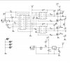
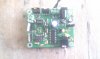
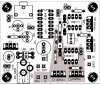
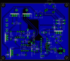
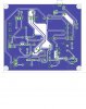
i need help i have the schemetics but i want some one to tele the schemetics and make a layout for me as short of time left for my demo presenting which is after 12 hrs this is a system about an audio amplifier which runs ultrasonic transducer which include IRF540 MOSFETS , IR2111 Half Bridge and TL494 IC and 7812 Voltage Regulator and some resistors and capacitor the schemetics is ready but learning how to convert it to layout take too much time while i have short time left the schemetics and original diagram is attached. Please tele if any mistake correct them and make a PCB layout for me which can be printed soon
 

Attachments

  • Direct1.JPG
    Direct1.JPG
    52.5 KB · Views: 3,597
  • pcb.sch
    207 KB · Views: 404
The problem is that there is no bill of material so there is no way to know, for example, what connector to put in the layout.
What is the second file (pcb.sch)
 
2P termianls to put in here like attached is one of the top veiwe of the circuit that was made but now its not working thats y i am redesigning it. and pcb.sch is the file that i have replaced the items with like ic4 it was in layout execise a transistor while it is a voltage regulator. so i need some one to make the layout for me.
 

Attachments

  • IMAG0151.jpg
    IMAG0151.jpg
    361.5 KB · Views: 582
its effort but i have lot of work to do now , preparation of presetation and its learning , learing concepts and making pcb so learnig now will be a bit tough need a layout any one please help :-(
 
Your schematic design is a desaster!

There are unconnected pins and parts do not have a value which makes it almost impossible to track the errors.

How should one get along with that kind of work if it's not his own design?

Don't change grids using odd numbers! Always use inch based grids and fractions of inches. Changing from grid size 1/10" (2.54mm) to any odd value, e.g. 1.26mm instead of 1.27 the nets will not connect properly.

Error tracking can be made by using the eye-symbol to highlight every net from beginning to end with all pins which should be connected. If one pin is not highlighted it won't be connected on the PCB layout.

Additionally the voltage regulator and all power MosFets are horizontally arranged (instead of vertically) on the PCB taking up a lot more space than on your photo.

Most of the capacitors used are tantalum type caps. There are lots of ceramic caps on the photo, but none in your design.

What's the second 8pin DIP IC?

Sorry, I can't help you now. Provide a better schematic and I'll see what I can do for you.

Boncuk
 
Last edited:
the circuit the component list and the sch file is attached please help me improving the circuit in making layout for me. the 8 pin IC is(IR2111) and the 7812 IC is the voltage regulator the 16 pin IC is TL494 and MOSFETS are IRF540 and some capacitor and resistors please help me making an accurate design. Everything is attached except the layout.
 

Attachments

  • Direct1.JPG
    Direct1.JPG
    52.5 KB · Views: 730
  • Direct3.JPG
    Direct3.JPG
    64.3 KB · Views: 528
  • IMAG0151.jpg
    IMAG0151.jpg
    361.5 KB · Views: 367
  • pcb.sch
    207 KB · Views: 272
How do you make an accurate PCB design if the faulty schematic still exists?

I do not intend to correct the schematic a way to put the blame on me in case the circuit won't work!

Follow all nets from beginning to end and all pins supposed to be connected to the nets.

At a glance I discovered two serious errors: The drain of Q3 has the net name N$39 ending in the middle of nowhere. The drain of Q1 is connected to net N$40 which is supposedly N$39, leading to fuse F1. You should know if the nets have to be the same.

GND should supposedly be connected to the source of Q2, but the net name changes from GND to N$19 with no ground connection! FATAL ERROR!

GYST and I really do what I can. Searching for net mismatches and unconnected pins will take more time than you have left over for your presentation!

I suggest to redraw the entire schematic (omitting nets drawn through the symbol of a device) asap and give me a call via Skype as soon as you have finished the design.

Boncuk

P.S. My hourly rate is US$350 to track errors in a schematic design. :mad:

And please! Use a frame format fitting the schematic design without having to alter the frame. DIN-A4 (landscape) is more than generous, not DIN-A3!

Instead of trying to create a schematic layout it would have been better to send me detailed photos of the original design for reverse engineering.
 
Last edited:
can u help me drawing the schemetics on skype my id is (khushal_kkk) please help me shall be thankful because i am so in need of this and cant draw myself and no one is helping me and m out of my mind and cant understand what u r saying :-( pls give me skype id or add me so i could talk to u and solve the issue
 
@Boncuk :
the 3 files are attached the Schemetics + Original Circit + Component List ...

TL494 IC
IR2111 IC
7812 Volatage Regulator
IRF540 MOSFET

and some resistors and capacitors
 

Attachments

  • Direct3.JPG
    Direct3.JPG
    64.3 KB · Views: 381
  • pcb.sch
    207 KB · Views: 191
  • Direct1.JPG
    Direct1.JPG
    52.5 KB · Views: 1,126
some more idea from the pic
 

Attachments

  • Direct Making.doc
    470 KB · Views: 283
  • IMAG0151.jpg
    IMAG0151.jpg
    361.5 KB · Views: 310
  • Direct2.JPG
    Direct2.JPG
    64.8 KB · Views: 972
Last edited:
Hi khushal,

since you're offline I post the PCB design here.

Perform "Ratsnest" before printing the board. This is important because of the ground fill.

I had to redraw the schematic as well.

Before you go to print the PCB layout compare your schematic with mine.

Regards

Boncuk
 

Attachments

  • AMP.gif
    AMP.gif
    28.8 KB · Views: 456
  • AMP.zip
    16.2 KB · Views: 202
no question about Boncuk's design.. Mr.kushal you can proceed with assembling
 
Last edited:
thank you for the help Boncuk and i am very pleased that there was some one who helped me alot and invested alot of time for me and i am very thnkful to you sir will never forget you in my prayers sir. God give u more and more happiness :)
 
Hi khushal,

I'm happy if I have made someone else happy. :)

I just hope that this little gesture of friendship will prevail throughout islamic and christian nations for a better mutual understanding.

Not that I'm afraid of war - I was a "cold warrior" for 23 years of my life until the Sowjet Union broke to pieces.

Allah or God or who ever may bless you.

Kindest regards

Boncuk
 
Last edited:
Aftr all now i know u are a strong man :) because in mid i saw ur anger just like soldiers nd i love the way u treat humanity , may God bless u sir nd offcorse this will help alot in bringing some muslims nd cristians nearer nd nearer atleast me :) nd yes sir i did checked the schemetics its exactly the same ive gven in jpeg format .
 
sir can u go through the circuit diagram please there is a little mistake in that the DC jack i need is attached , and the diodes connected to dc jack are connected to one pin instead of goin to seperate pins
2) the pads GNDA is with A and GNDB is with B because there connects the 2p Termianls.

i dont know how to fix sir please can u do that for me
 

Attachments

  • dc jack.JPG
    dc jack.JPG
    144.5 KB · Views: 410
Status
Not open for further replies.

New Articles From Microcontroller Tips

Back
Top