We start with the SPI bus... The main idea behind serial buses is to save on micro-controller pins... SPI requires three pins or more if there are multiple devices.. The serial transfer on an SPI bus is circular.. The inputs and outputs of each buffer are connected and the shift is synchronized.

As data is shifted out of the SDO pin of a micro, the data is shifted into the SDI pin of the device...The data in the device is simultaneously shifted back into the micro. When large data transfers are made after the first (dummy) data is read, the next byte will be called data, this means you can swap chunks of data back and forth relativity quickly... Some SPI buses can run at 10Mbit per second...
Multiple devices are addressed using a Chip Select (CS) pin.... There are certain devices that are software addressable making the need of the CS pin obsolete, but not many! For the examples I use hardware addressing which usually means supplying a CS pin per device.
The protocol for talking to SPI devices is fairly simple.. 8 clocks to shift the buffers round whilst holding the CS pin low...
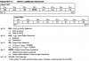
There are 4 modes of operation and most devices will work with at least two, the modes are determined by the clock signal...
Normally Low with Rising Clock Mode 0,0 / Mode 0
Normally Low with Falling Clock Mode 0,1 / Mode 1
Normally High with Rising Clock Mode 1,0 / Mode 2
Normally High with Falling Clock Mode 1,1 / Mode 3
Each device has a datasheet ( somewhere on the net ) that will describe the operation... Micro's with hardware SPI modules have a register where this can be set. However! We are going to implement a software bit banged one so we'll have to take it into consideration.
The devices I'm going to use are the ADC and the DAC. For the DAC I use the MCP4921 and the MCP3001 for the ADC..
The MCP4921 is a 12 bit DAC.... So our output has 4096 resolutions, that means for a 0v ~ 5v span we will see changes a little as 1.2mV... To output a voltage we have to load the DAC via the SPI pins... There is 12bits for the DAC itself and 4 bits for control.
Here is the register inside the DAC as displayed in the relevant datasheet..

From this we can see we need 2 x 8 bit data transfers..
Bit 15 is only used on the dual MCP4922.
Bit 14 is for the internal buffer, this is used when updating the DAC causes loading issues.
Bit 13 is the gain control, it set it uses the ref pin as its span if unset it uses the ref pin and doubles( if it can ) the output.... If the DAC runs on 5v this will be the cap.. It cannot be used as a voltage doubler.. Most people use a precision 1.2v or 2.5v reference... This means they can double the output to 2.4v and 5v respectively..
Bit 12 is the shutdown control.
When we write to the DAC we need to add 0x3000 to the DAC value so the chip will be enabled and we can use a 5v reference.
The MCP3001 has a slightly different protocol than the DAC... This being a 10bit ADC there are only 11 bits to shift out.. 1 NULL bit and then the 10 ADC result bits.. There are no control bits..
If we read 16 clocks the first two clocks receive nothing... The 3rd clock receives the NULL bit and the following 10 clocks receive the data.. The last few clocks can be discarded... As we will be using a software SPI implementation for both chips then the full 16 bits will be being used. This way if an upgrade to hardware SPI is required, little software changes will be needed..
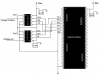
Ok! We need a circuit.

I haven't included( as usual ) the connections to the bootloader.. This is an addon to the basic circuit shown in the first tutorial... Also as we are dabbling with ADC's and DAC's we need to ensure decoupling caps are on all chips... 0.1uf is the usual cap to use... These must be placed as close to the power pins as possible...
I'll show the ASM code first so we can see it in action... I'm going to read a pot connected to the MCP3001 and watch a voltmeter connected to the MCP4921...
Code 17
It works as expected...
Okay! The C version...
Code18
So you can see SPI isn't rocket science DATA is shifted out by the most significant bit whilst DAT is shifted in on the least significant bit.. This really speeds up the operation.
The other major contender for inter device communication is I2C..
Inter IC Communication. Shortened to.. I squared C ( I2C )..
I2C is pretty much the same as SPI but has only two wire hookup, hence why some call it two wire communication.. The master controls up to 128 devices.. Each device has an internal address... This allows us to leave out the Chip Select pins....
If an I2C bus has several similar devices they must have external code switches...
An 24LC256 eeprom has an internal address of 0x50... But! As the address has to include a R/W bit we need to shift the address into a byte so the address becomes 0xA0 for writing and 0xA1 for reading..
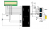
For our example, I'll use a 24LC256 eeprom coupled with DS1307 RTC... We will have to bring back the LCD routines so we can see stuff on the screen ( otherwise nothing will look like its happening ).
First thing as before.. A schematic.. We need to know how to connect it up.. I normally hook stuff up to port 1, but I have the LCD on there.... I have use Port 0 pins 6 and 7..
As we only have one 24lc256 the three address lines are grounded...

I have included a file or two... This is helpful when making large programs.. Take all your code and bundle it in a file.... Call it MyLibrary.C or something else that fits the bill... Name all your function definitions and constants and place it in a file called MyLibrary.H or similar... Now when you include any functions from the library, then only these will be included in the build..
But before the version I'll start with ASM as usual..
Code19
The include file (I2C,inc) has all the low level code... I will stick it in the appendix and include it on the forum.
Code20
And there in lies software SPI and I2C routines
I have included the two files... I2C.inc for the ASM code ( rename from I2C.h)
and the MyLibrary.H for the C code ( My compiler wont allow multiple C files so I have done it as a header!!! Same difference)..
I'm on with the Graphical display now.... I'll try and get it posted soon..
As data is shifted out of the SDO pin of a micro, the data is shifted into the SDI pin of the device...The data in the device is simultaneously shifted back into the micro. When large data transfers are made after the first (dummy) data is read, the next byte will be called data, this means you can swap chunks of data back and forth relativity quickly... Some SPI buses can run at 10Mbit per second...
Multiple devices are addressed using a Chip Select (CS) pin.... There are certain devices that are software addressable making the need of the CS pin obsolete, but not many! For the examples I use hardware addressing which usually means supplying a CS pin per device.
The protocol for talking to SPI devices is fairly simple.. 8 clocks to shift the buffers round whilst holding the CS pin low...
There are 4 modes of operation and most devices will work with at least two, the modes are determined by the clock signal...
Normally Low with Rising Clock Mode 0,0 / Mode 0
Normally Low with Falling Clock Mode 0,1 / Mode 1
Normally High with Rising Clock Mode 1,0 / Mode 2
Normally High with Falling Clock Mode 1,1 / Mode 3
Each device has a datasheet ( somewhere on the net ) that will describe the operation... Micro's with hardware SPI modules have a register where this can be set. However! We are going to implement a software bit banged one so we'll have to take it into consideration.
The devices I'm going to use are the ADC and the DAC. For the DAC I use the MCP4921 and the MCP3001 for the ADC..
The MCP4921 is a 12 bit DAC.... So our output has 4096 resolutions, that means for a 0v ~ 5v span we will see changes a little as 1.2mV... To output a voltage we have to load the DAC via the SPI pins... There is 12bits for the DAC itself and 4 bits for control.
Here is the register inside the DAC as displayed in the relevant datasheet..
From this we can see we need 2 x 8 bit data transfers..
Bit 15 is only used on the dual MCP4922.
Bit 14 is for the internal buffer, this is used when updating the DAC causes loading issues.
Bit 13 is the gain control, it set it uses the ref pin as its span if unset it uses the ref pin and doubles( if it can ) the output.... If the DAC runs on 5v this will be the cap.. It cannot be used as a voltage doubler.. Most people use a precision 1.2v or 2.5v reference... This means they can double the output to 2.4v and 5v respectively..
Bit 12 is the shutdown control.
When we write to the DAC we need to add 0x3000 to the DAC value so the chip will be enabled and we can use a 5v reference.
The MCP3001 has a slightly different protocol than the DAC... This being a 10bit ADC there are only 11 bits to shift out.. 1 NULL bit and then the 10 ADC result bits.. There are no control bits..
If we read 16 clocks the first two clocks receive nothing... The 3rd clock receives the NULL bit and the following 10 clocks receive the data.. The last few clocks can be discarded... As we will be using a software SPI implementation for both chips then the full 16 bits will be being used. This way if an upgrade to hardware SPI is required, little software changes will be needed..
Ok! We need a circuit.
I haven't included( as usual ) the connections to the bootloader.. This is an addon to the basic circuit shown in the first tutorial... Also as we are dabbling with ADC's and DAC's we need to ensure decoupling caps are on all chips... 0.1uf is the usual cap to use... These must be placed as close to the power pins as possible...
I'll show the ASM code first so we can see it in action... I'm going to read a pot connected to the MCP3001 and watch a voltmeter connected to the MCP4921...
Code 17
Code:
$MOD51

ResultL    equ   31H     ; Low byte
ResultH    equ   30H     ; High byte

   org    0
   ljmp   Start     ; jump over vectors

   org    30H
Start:   call   SPIInit     ; Ready for SPI

Main:
   call    GetVal     ; Read ADC
   call   SendVal     ; Convert to 12 bit
   sjmp    Main     ; And send to DAC

; The MCP3001 is a 10 bit ADC but the split over the two
; registers is weird
; x,x,x,null,D9,D8,D7,D6,D5,D4,D3,D2,D1,D0,D1,D2,D3

GetVal:
   clr   P1.4     ; CS enable
   mov   A,#0
   call   doSPI     ; Clock in ADC
   mov   ResultH,A   ; Get ADC high
   mov   A,#0
   call   doSPI     ; Clock in ADC
   mov   ResultL,A   ; Get ADC low
   setb   P1.4     ; CS disable
   mov   R0,#2     ; Shift out 2 bits

; Next bit removes all rubish and makes a 12 bit result..

shift:   clr   C     ; clear carry before shift
   mov   A,ResultH   ; shift High into Acc
   rrc   A     ; rotate with carry
   mov   ResultH,A   ; store back
   mov   A,ResultL   ; low byte into Acc
   rrc   A     ; rotate with carry
   mov   ResultL,A   ; store back
   djnz   R0,shift   ; All 4 bits
   mov   A,ResultH   ; Get High byte
   anl   A,#0fh     ; Trim to 12 bits
   mov   ResultH,A   ; Store back
   ret

; Send 12 bit result to the MCP4921..

SendVal:
   clr   P1.3     ; CS enable
   mov   A,ResultH   ; get High byte
   add   A,#30h     ; set control bits
   call   doSPI     ; send out
   mov   A,ResultL   ; get low byte
   call   doSPI     ; send out
   setb   P1.3     ; CS dissable
   ret

; Ready the pins for SPI transfers

SPIInit:
   mov   P1,#0ffH   ; Port 1 as input
   clr   P1.6     ; Clock low idle
   ret

; Do the SPI transfer

doSPI:   clr   C     ; Clear carry
   mov   R0,#8     ; 8 clocks
LpIn:   clr   P1.5
   jnb   Acc.7,BBit   ; bit 7? high / low
   setb   P1.5     ; high
BBit:   call   Clock     ; low and clock
   jnb   P1.7, None   ; Whats come in???
   setb   C     ; High
   jmp   ABit
None:   clr   C     ; or Low
ABit:   rlc   A     ; next bit
   djnz    R0,LpIn     ;
   ret

; Clock the SCL line

Clock:
   setb   P1.6     ; Clock
   nop       ; Wait
   clr   P1.6     ; Scl pin
   ret

endOkay! The C version...
Code18
C:
/* Main.c file generated by New Project wizard
 *
 * Created:  Thu Apr 16 2015
 * Processor: AT89C51RB2
 * Compiler:  SDCC for 8051
 */

#include <mcs51reg.h>
#define   SDO P1_5
#define   SDI P1_7
#define   SCL P1_6
#define   CSA P1_4
#define   CSD P1_3

void SPIinit(void)
  {
  P1 = 0xBF;      // Clock idle low
  }

unsigned char doSPI(unsigned char CH)
  {
  char Idx;

  for (Idx = 0; Idx<8;Idx++)
  {
  SDO = 0;
  if(CH & 0x80) SDO = 1;
  SCL = 1;
  SCL = 0;
  CH <<= 1;
  CH &= 0xFE;
  if(SDI == 1) CH++;
  }
  return CH;
  }

int ReadADC(void)
  {
  int tmp = 0;
  CSA = 0;
  tmp = (int)doSPI(0);
  tmp <<= 8;
  tmp += (int)doSPI(0);
  CSA = 1;
  tmp>>= 2;
  return tmp & 0xFFF;
  }

void WriteDAC(int x)
  {
  x += 0x3000;
  CSD = 0;
  doSPI(x >> 8);
  doSPI(x & 0xFF);
  CSD = 1;
  }

void main(void)
 {
  // Write your code here
  while (1)
  {
  WriteDAC(ReadADC());
  }
}The other major contender for inter device communication is I2C..
Inter IC Communication. Shortened to.. I squared C ( I2C )..
I2C is pretty much the same as SPI but has only two wire hookup, hence why some call it two wire communication.. The master controls up to 128 devices.. Each device has an internal address... This allows us to leave out the Chip Select pins....
If an I2C bus has several similar devices they must have external code switches...
An 24LC256 eeprom has an internal address of 0x50... But! As the address has to include a R/W bit we need to shift the address into a byte so the address becomes 0xA0 for writing and 0xA1 for reading..
For our example, I'll use a 24LC256 eeprom coupled with DS1307 RTC... We will have to bring back the LCD routines so we can see stuff on the screen ( otherwise nothing will look like its happening ).
First thing as before.. A schematic.. We need to know how to connect it up.. I normally hook stuff up to port 1, but I have the LCD on there.... I have use Port 0 pins 6 and 7..
As we only have one 24lc256 the three address lines are grounded...
I have included a file or two... This is helpful when making large programs.. Take all your code and bundle it in a file.... Call it MyLibrary.C or something else that fits the bill... Name all your function definitions and constants and place it in a file called MyLibrary.H or similar... Now when you include any functions from the library, then only these will be included in the build..
But before the version I'll start with ASM as usual..
Code19
Code:
sec   equ   30h
min   equ   31h
hour   equ   32h
day   equ   33h
date   equ   34h
mon   equ   35h
year   equ   36h

   org   0
   sjmp   start
   org   30h

start:   acall   i2cinit
   acall   LcdInit
   acall   settime
   mov   R3,#1
   mov   R2,#0
   mov   R1,#0AAh
   acall   writeEEprom
   acall   delay
   mov   R1,#0
   acall   readEEprom

main:
   acall   gettime
   acall   printRTC
   sjmp   main

t_data:   db   0h,23h,13h,0h,17h,4h,15h

printRTC:
   acall   LcdGotoline1
   mov   R0,#hour
   mov   A,@R0
   dec   R0
   acall   printhex
   mov   A,#3Ah
   call    lcdData
   mov   A,@R0
   dec   R0
   acall   printhex
   mov   A,#3Ah
   call    lcdData
   mov   A,@R0
   acall   printhex
   acall   LcdGotoline2
   mov   R0,#date
   mov   A,@R0
   inc   R0
   acall   printhex
   mov   A,#2fh
   call    lcdData
   mov   A,@R0
   inc   R0
   acall   printhex
   mov   A,#2fh
   call    lcdData
   mov   A,@R0
   acall   printhex
   mov   A,#20h
   call    lcdData
   ret

printhex:
   push   Acc
   swap   A
   anl   A,#0fh
   add   A,#30h
   call    lcdData
   pop   Acc
   anl   A,#0fh
   add   A,#30h
   call    lcdData
   ret

gettime:
   mov   R0,#7
   mov   R2,#0
   mov   R1,#sec
idx2:   acall   readRTC
   mov   A,R3
   mov   @R1,A
   inc   R2
   inc   R1
   djnz   R0,idx2
   ret

settime:
   mov   R0,#7
   mov   R2,#0
   mov   dptr,#t_data
idx1:   mov   A,#0h
   movc   A,@a+dptr
   mov   R3,A
   acall   writeRTC
   inc   R2
   inc   dptr
   djnz   R0,idx1
   ret

$include   (I2C.inc)
   end
The include file (I2C,inc) has all the low level code... I will stick it in the appendix and include it on the forum.
Code20
C:
/* Main.c file generated by New Project wizard
 *
 * Created:  Fri Apr 17 2015
 * Processor: AT89C51RB2
 * Compiler:  SDCC for 8051
 */

#include <mcs51reg.h>
#include <stdio.h>
#include "MyLibrary.H"

unsigned char output[17];
unsigned char time[] = {0x0,0x3,0x17,0x0,0x17,0x4,0x15};

void WriteClock(char *array)  // Not used
  {
  char x;
  for(x=0;x<7;x++)
  {
  WriteRTC(x,array[x]);
  }
  }

void ReadClock(char *array)
  {
  char x;
  for(x=0;x<7;x++)
  array[x] = ReadRTC(x);  // No need to BCD-BIN
  }

void main(void)
 {
  I2Cinit();
  lcd_init();
  WriteClock(&time[0]);
  while (1)
  {
  lcd_command(0x80);
  ReadClock(&time[0]);
  sprintf(output,"%02x:%02x:%02x",time[2],time[1],time[0]);
  lcd_print(output);
  lcd_command(0xC0);
  sprintf(output,"%02x/%02x/%02x",time[4],time[5],time[6]);
  lcd_print(output);
  }
 }
And there in lies software SPI and I2C routines
I have included the two files... I2C.inc for the ASM code ( rename from I2C.h)
and the MyLibrary.H for the C code ( My compiler wont allow multiple C files so I have done it as a header!!! Same difference)..
I'm on with the Graphical display now.... I'll try and get it posted soon..