Continue to Site

Welcome to our site!

Electro Tech is an online community (with over 170,000 members) who enjoy talking about and building electronic circuits, projects and gadgets. To participate you need to register. Registration is free. Click here to register now.

  • Welcome to our site! Electro Tech is an online community (with over 170,000 members) who enjoy talking about and building electronic circuits, projects and gadgets. To participate you need to register. Registration is free. Click here to register now.

Temperature controlled fan using PIC16F877a (in assembly language)

bobabey

New Member
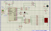
Hello! im doing a simulation mini project (temperature controlled fan) using PIC16F877A on Proteus and MPLAB IDE V8 for coding. i need help with my assembly code. i think there is something wrong with the temperature code section/AD conversion? i have due in a week :( PLEASE HELP ME. Below is the details of the project:

Temperature controlled fan operations:
- LM35 as input for sensing temperature
- If start button pressed momentarily, system operation starts.
- if stop button pressed momentarily, all operation stop.
- 0-39°C (low temp) fan motor off, LED off, buzzer off and 7 segment display '0' indicate low temp.
- 40°C above (high temp) fan motor on, LED on, buzzer on and 7 segment display '1' indicate high temp.

Code:
;EQUATES SECTION

TMR0        EQU    1        ; TMR0 register
STATUS        EQU    3        ; STATUS register
PORTA        EQU    5        ; PORTA register
PORTB        EQU    6        ; PORTB register
PORTC        EQU    7
PORTD        EQU    8
PORTE        EQU    9
TRISA        EQU    85H        ; TRISA register address
TRISB        EQU    86H        ; TRISB register address
TRISC        EQU    87H
TRISD        EQU    88H
TRISE        EQU    89H
OPTION_R    EQU    81H        ; OPTION Register address
INTCON        EQU    0BH        ;Interrupt Control Register
GIE            EQU    7        ;Global Interrupt bit
INTE        EQU    4        ;B0 Interrupt Enable bit
INTF        EQU    1        ;B0 Interrupt Flag
ADCON0        EQU    1FH    ; A/D Configuration register 0
ADCON1        EQU    9FH    ; A/D Configuration register 1
ADRES        EQU    1EH    ; A/D Result register
CHS0        EQU    3        ; Channel select bit
GODONE        EQU    2        ; A/D Conversion Status bit
CARRY        EQU    0        ; Carry bit
ZEROBIT        EQU    2        ; Zero bit
COUNT        EQU    20H    ; COUNT register address
COUNTA        EQU    21H    ; COUNTA register address
TMR0_T        EQU    22H    ; Temporary register for TMR0
W_TEMP        EQU    23H    ; Temporary W register
STATUS_T    EQU    24H    ; Temporary STATUS register
PORTB_T        EQU    25H    ; Temporary PORTB register

;*****************************************************************************

    LIST    P=16F877A    ; Using 16F877 microcontroller
    ORG    0            ; Start address in memory
    GOTO    START

;*****************************************************************************

;CONFIGURATION BITS SECTION

    __CONFIG    H'3FF2'    ; HS oscillator, WDT off, PUT on, Code Protection disabled

;*****************************************************************************

;SUBROUTINE SECTION

; 10ms delay subroutine
DELAY    CLRF    TMR0            ; Clear TMR0
LOOPA    MOVF    TMR0, W            ; Move TMR0 to W
        SUBLW    .195            ; Subtract 195 from W
        BTFSS    STATUS, ZEROBIT    ; Check if result is zero
        GOTO    LOOPA            ; If not zero, repeat loop
        RETLW    0                ; If zero, return

;0.5sec delay
DELAYP5    MOVLW    .50                    ;W = 50
        MOVWF    COUNTA                ;W put inside file COUNTA
LOOPC    CALL    DELAY                ;goto delay
        DECFSZ    COUNTA                ;COUNTA - 1 = COUNTA
        GOTO    LOOPC                ;goto LOOPC
        RETLW    0                    ;COUNTA is 0, return

;1sec delay
DELAY1    MOVLW    .100                ;W = 100
        MOVWF    COUNT                ;W put inside file COUNT
LOOPB    CALL    DELAY                ;goto delay
        DECFSZ    COUNT                ;COUNT - 1 = COUNT
        GOTO    LOOPB                ;goto LOOPB
        RETLW    0                    ;COUNT is 0, return

COND1    BCF        PORTB, 5
        MOVLW   B'00000000'       ;set RA1 and RA2 high to turn on CP1 and CP2 LEDs
        MOVWF   PORTC              ;CP1 and CP2 LEDs turned on
         MOVLW   .0               ;load literal '0' to W register 
        MOVWF   PORTD            ;Display '0' on 7-segment display for all parks full
        RETLW    0

COND2    BSF        PORTB, 5
        MOVLW   B'00001001'       ;set RA1 and RA2 high to turn on CP1 and CP2 LEDs
        MOVWF   PORTC              ;CP1 and CP2 LEDs turned on
        MOVLW   .1               ;load literal '0' to W register 
        MOVWF   PORTD            ;Display '0' on 7-segment display for all parks full
        RETLW    0

;*****************************************************************************

;CONFIGURATION SECTION

START    BSF        STATUS, 5            ; Set bank to access TRISA and TRISB

    ; Configure PORTA and PORTB
    MOVLW    B'11111111'            ; PORTA as input
    MOVWF    TRISA

    MOVLW    B'00000000'
    MOVWF    ADCON1        ;all PORTA are analogue

    MOVLW    B'00000011'            ; PORTB as output
    MOVWF    TRISB

    MOVLW    B'00000000'
    MOVWF    TRISC
    
    MOVLW    B'00000000'
    MOVWF    TRISD

    MOVLW    B'00000000'
    MOVWF    TRISE

    ; Configure A/D Converter
    ;MOVLW    B'00000001'            ; PORTB,0 as input for A/D Converter
    ;MOVWF    TRISB
    ;MOVLW    B'00000000'            ; Set A/D Control Register 1 for analog input
    ;MOVWF    ADCON1

    ; Set up Timer0 for delay
    MOVLW    B'00000111'            ; Prescaler is /256
    MOVWF    OPTION_R

    BCF        STATUS, 5            ; Return bank to 0
    CLRF    PORTA                    ; Clear PORTA
    CLRF    PORTB                    ; Clear PORTB
    CLRF    PORTC
    CLRF    PORTD
    CLRF    PORTE
    CLRF    COUNT
    CLRF    COUNTA

    ; Turn on A/D Converter and enable interrupts
    BSF        ADCON0, 0            ; Turn ON A/D

;*****************************************************************************

;PROGRAM STARTS NOW

;SWITCH 1
MAIN    BTFSS   PORTB, 0          ;check if SW1 to start the operation is pressed (active low) 
        GOTO    BEGIN            ;if pressed, go to begin
        GOTO    MAIN            ;if not pressed, wait for SW1 to be pressed
              
;SWITCH 2           
BEGIN    BTFSS   PORTB, 1          ;check if SW2 to stop the operation is pressed (active low)
        GOTO    STOP            ;if pressed, go to stop

TEMP    BSF        ADCON0, CHS0        ;C to select A0
        BSF        ADCON0, GODONE    ;Measures temperature from AO, Set GO/DONE

WAIT    BTFSC    ADCON0, GODONE    ;Wait until GO/DONE is clear
        GOTO    WAIT            ;temperature loop in A/D reg. ADRES

        MOVF    ADRES, W            ;Move ADRES file content to W
        SUBLW    .82       
        BTFSC    STATUS, CARRY   
        GOTO    LOWTEMP
        GOTO    HITEMP        ; Otherwise, go to TEMP_ABOVE subroutine
        
    
LOWTEMP    CALL    COND1
        GOTO    BEGIN
        
HITEMP    CALL    COND2
        GOTO    BEGIN

;SWITCH 2 STOP OPERATION
STOP    BCF     PORTB, 5         ;set RA1 low to turn off CP1 LED
        MOVLW   B'00000000'       ;set RA1 and RA2 high to turn on CP1 and CP2 LEDs
        MOVWF   PORTC              ;CP1 and CP2 LEDs turned on
        MOVLW   .0               ;load literal '0' to W register
        MOVWF   PORTD            ;Display '0' on 7-segment display for stop operation
        GOTO    MAIN             ;restart operation
        
        END
 

Attachments

  • CIRCUIT DIAGRAM.png
    CIRCUIT DIAGRAM.png
    83.4 KB · Views: 43
On the PIC16F877A, the A2D has two separate phases of operation. First there is acquisition then there is conversion. The software has to put the A2D into acquisition mode and then leave it for enough time before initiating conversion and waiting for that to finish. When that is finished the A2D registers can be read.

That process is repeated for each reading.

You have set TRISB twice. It has nothing to do with the A2D but the comments say that it is.

I don’t know what the oscillator frequency is, so I don’t know what frequency the A2D is being clocked at. That frequency has to be 600 kHz or less. Normally that means that the A2D divide ratio should be 16 or 32, which is set by various bits in the A2D configuration registers.
 
Based on your posted code I have some doubt that you could learn enough in less than a week to create a working example.

Do you want someone to do your assignment for you?
 
I doubt that the Original Poster will check to see if an answer was ever posted.

This code has never been tested with the Proteus simulator or real hardware for that matter.

Code:
        list    p=16F877A       ; Select PIC16F877A as target device
        list    n=0, c=250      ; No page breaks, support long lines in list file
        list    r=dec
        errorlevel -302         ; Suppress not in bank zero warning
#include <p16f877A.inc>
;
; Configuration words.
; Define these in just one file.
;
        __CONFIG _FOSC_HS & _WDTE_OFF & _PWRTE_OFF & _BOREN_OFF & _LVP_OFF & _CPD_OFF & _WRT_OFF & _CP_OFF
;
; Define macros to help with
; bank selection
;
#define BANK0  (h'000')
#define BANK1  (h'080')
#define BANK2  (h'100')
#define BANK3  (h'180')
;
; File: main.asm
; Target: PIC16F877A
; IDE: MPLAB v8.92
; Compiler: MPASMWIN v5.51
;
; -------------------------
; Main application
; -------------------------
;
;                         PIC16F877A
;                 +----------:_:----------+
;       VPP ->  1 : MCLR/VPP      PGD/RB7 : 40 <> PGD
;      LM35 ->  2 : RA0/AN0       PGC/RB6 : 39 <> PGC
;           <>  3 : RA1               RB5 : 38 <> FAN_ON
;           <>  4 : RA2               RB4 : 37 <>
;           <>  5 : RA3           PGM/RB3 : 36 <>
;           <>  6 : RA4               RB2 : 35 <>
;           <>  7 : RA5               RB1 : 34 <> SW2
; CD4511_LE <>  8 : RE0               RB0 : 33 <> SW1
;           <>  9 : RE1               VDD : 32 <- PWR
;           <> 10 : RE2               VSS : 31 <- GND
;       PWR -> 11 : VDD               RD7 : 30 <>
;       GND -> 12 : VSS               RD6 : 29 <>
;     20MHZ -> 13 : OSC1              RD5 : 28 <>
;     20MHz <- 14 : OSC2              RD4 : 27 <>
;       LED <> 15 : RC0/SOSCO   RX/DT/RC7 : 26 <>
;           <> 16 : RC1/SOSCI   TX/CK/RC6 : 25 <>
;           <> 17 : RC2/CCP1          RC5 : 24 <>
;    BUZZER <> 18 : RC3/SCL       SDA/RC4 : 23 <>
; CD4511_A  <> 19 : RD0               RD3 : 22 <> CD4511_D
; CD4511_B  <> 20 : RD1               RD2 : 21 <> CD4511_C
;                 +-----------------------:
;                          DIP-40
;
;
;------------------------------------------------------------------------
RESET_VECTOR CODE 0x000                     ; processor reset vector
        nop                                 ; ICD2 needs this NOP
        goto    start                       ; begin PIC initialization

;------------------------------------------------------------------------
;
; This applicaiton does not use interrupts
;
INT_VECTOR code 0x004                       ; interrupt vector location

INTERRUPT:
        retfie                              ; return from interrupt
;------------------------------------------------------------------------
start:
    clrf    INTCON              ; Disable all interrupt sources
    banksel BANK1
    clrf    PIE1
    clrf    PIE2

    movlw   b'11000001'         ; Pull-ups off, INT edge low to high, WDT prescale 1:1
    movwf   OPTION_REG          ; TMR0 clock edge low to high, TMR0 clock = FCY, TMR0 prescale 1:4
                                ; TIMER0 will assert the overflow flag every 256*4 (1024) instruction
                                ; cycles, with a 20MHz oscilator this is every 0.2048 milliseconds.

    movlw   b'11111111'         ;
    movwf   TRISA

    movlw   b'11011111'         ; RB5:FAN_ON
    movwf   TRISB

    movlw   b'11110110'         ; RC3:BUSSER, RC0:LED
    movwf   TRISC

    movlw   b'11110000'         ; RD3-RD0:CD4511_D-CD4511_A
    movwf   TRISD

    movlw   b'00000110'         ; RE0:CD4511_LE
    movwf   TRISE

    ; disable comparators
    movlw   b'00000111'
    movwf   CMCON

    ; Set RA0/AN0 as ADC input, all others are for digital I/O
    movlw   b'10001110'         ; Right justified data
    movwf   ADCON1

    banksel BANK0
    movlw   b'11000001'         ; FRC as ADC clock, Channel AN0, ADC on
    movwf   ADCON0
    clrf    TMR0
 
    pagesel main
    goto    main
;
;
;
MAIN_DATA udata
; Note: Application does not use any RAM at present

MAIN_CODE code

main:
    banksel BANK0
    clrf    PORTB
    clrf    PORTC
    movlw   b'11111111'
    movwf   PORTD
    clrf    PORTE

AppLoop:
    btfsc   PORTB,0         ; skip if start switch is pressed
    goto    AppLoop
;
; Start fan control
FanLoop:
    btfss   PORTB,1         ; skip if stop switch is not pressed
    goto    main

;
; Wait for TIMER0 to assert at least once
    btfss   INTCON,TMR0IF
    goto    $-1
    bcf     INTCON,TMR0IF
    btfss   INTCON,TMR0IF
    goto    $-1

;
; Do an ADC conversion
    bsf     ADCON0,GO_NOT_DONE
    btfsc   ADCON0,GO_NOT_DONE
    goto    $-1
;
; Counts_Per_volt = ADC_MAX / VREF
; Temp_volts      = 40C * 0.01 volts
; ADC trip point  = Temp_volts * Counts_Per_volt
;                 = 0.4 * 1023 / 5.0
;                 = 81.84
;
#define ADC_TRIP_40c (D'80')
;
;   set CARRY flag when ADC result is less than or equal to ADC_TRIP_40c
    banksel BANK1
    movf    ADRESL,W

    sublw   LOW(ADC_TRIP_40c)
    banksel BANK0
    movf    ADRESH,W
    btfss   STATUS,C
    decfsz  ADRESH,W
    sublw   HIGH(ADC_TRIP_40c)
 
    btfsc   STATUS,C
    goto    LessThan40c
;
; Turn on fan
    movlw   B'00100000'
    movwf   PORTB           ; Turn on fan
    movlw   B'00001001'
    movwf   PORTC           ; Turn on LED and BUZZER
    movlw   1
    movwf   PORTD           ; Write 1 to 7-segment decoder

    goto    FanLoop
;
LessThan40c:
;
; Turn off fan
    movlw   B'00000000'
    movwf   PORTB           ; Turn off fan
    movlw   B'00000000'
    movwf   PORTC           ; Turn off LED and BUZZER
    movlw   0
    movwf   PORTD           ; Write 0 to 7-segment decoder

    goto    FanLoop

    END
 
Last edited:

New Articles From Microcontroller Tips

Back
Top